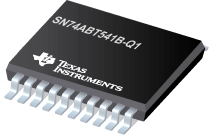
SN74ABT541B-Q1 具有三态输出的汽车类八路缓冲器/驱动器
 SN74ABT541B-Q1 描述
The SN74ABT541B octal buffer and line driver is ideal for driving bus lines or buffering memory address registers. The device features inputs and outputs on opposite sides of the package to facilitate printed circuit board layout.
The 3-state control gate is a two-input AND gate with active-low inputs so that if either output-enable OE1 or OE2) input is high, all eight outputs are in the high-impedance state.
When VCC is between 0 and 2.1 V, the device is in the high-impedance state during power up or power down. However, to ensure the high-impedance state above 2.1 V, OE should be tied to VCC through a pullup resistor; the minimum value of the resistor is determined by the current-sinking capability of the driver
| SN74ABT541B-Q1 | |
| Voltage Nodes(V) | 5 |
| Vcc range(V) | 4.5 to 5.5 |
| Logic | True |
| Input Level | TTL |
| Output Level | TTL |
| Output Drive(mA) | -32/64 |
| No. of Outputs | 8 |
| tpd max(ns) | 3.5 |
| Static Current | 30 |
| Rating | Automotive |
| Technology Family | ABT |
SN74ABT541B-Q1 特性
- Qualified for Automotive Applications
- ESD Protection Exceeds 2000 V Per MIL-STD-883, Method 3015; Exceeds 150 V Using Machine Model (C = 200 pF, R = 0)
- State-of-the-Art EPIC-IIB™ BiCMOS Design Significantly Reduces Power Dissipation
- Latch-Up Performance Exceeds 500 mA Per JEDEC Standard JESD-17
- Typical VOLP (Output Ground Bounce) <1 V at VCC = 5 V, TA = 25°C
- High-Impedance State During Power Up and Power Down
- High-Drive Outputs (–32-mA IOH, 64-mA IOL)
SN74ABT541B-Q1 芯片订购指南
| 器件 | 状态 | 温度 | 价格(美元) | 封装 | 引脚 | 封装数量 | 封装载体 | 丝印标记 |
| SN74ABT541BIPWRQ1 | ACTIVE | -40 to 85 | 0.59 | 1ku | TSSOP (PW) | 20 | 2000 |
SN74ABT541B-Q1 质量与无铅数据
| 器件 | 环保计划* | 铅/焊球涂层 | MSL 等级/回流焊峰 | 环保信息与无铅 (Pb-free) | DPPM / MTBF / FIT 率 |
| SN74ABT541BIPWRQ1 | Green (RoHS & no Sb/Br) | CU NIPDAU | Level-3-260C-168 HR | SN74ABT541BIPWRQ1 | SN74ABT541BIPWRQ1 |
SN74ABT541B-Q1 应用技术支持与电子电路设计开发资源下载
- SN74ABT541B-Q1 数据资料 dataSheet 下载.PDF
- TI 德州仪器缓冲器、驱动器/收发器产品选型与价格 . xls
- CMOS 非缓冲反向器在振荡器电路中的使用 (PDF 951 KB)
- Semiconductor Packing Methodology (PDF 3005 KB)
- 逻辑产品选择指南 2006/2007 (修订版 Z)(4462KB)
- 标准线性和逻辑产品 5 分钟指南 (786KB)
- 了解和解释标准逻辑数据表
- LOGIC Pocket Data Book (PDF 6001 KB)
- HiRel Unitrode Power Management Brochure (PDF 206 KB)
- Logic Cross-Reference (PDF 2938 KB)
