LTC1100 - Precision, Zero-Drift Instrumentation Amplifier
The LTC™1100 is a high precision instrumentation amplifier using zero-drift techniques to achieve outstanding DC performance. The input DC offset is typically 1µV while the DC offset drift is typically 5nV/°C; a very low bias current of 65pA is also achieved.
The LTC1100 is self-contained; that is, it achieves a differential gain of 100 without any external gain setting resistor or trim pot. The gain linearity is 20ppm and the gain drift is 4ppm/°C. The LTC1100 operates from a single 5V supply up to �8V. The output typically swings 300mV from its power supply rails with a 10k load.
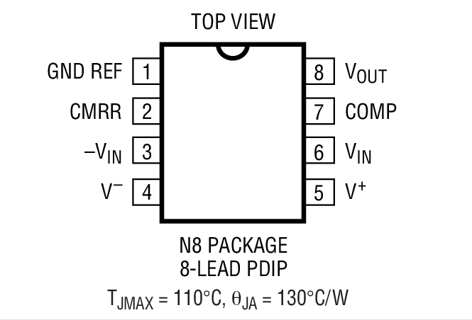
An optional external capacitor can be added from Pin 7 to Pin 8 to tailor the device�s 18kHz bandwidth and to eliminate any unwanted noise pickup.
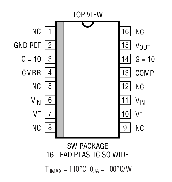
The LTC1100 is also offered in a 16-pin surface mount package with selectable gains of 10 or 100.
The LTC1100 is manufactured using Linear Technology’s enhanced LTCMOS®silicon gate process.
| 器件型号 | 封装 | 温度 | 价格 (以 1 ~ 99 片为批量) | 价格 (以 1000 片为批量) * |
|---|---|---|---|---|
| LTC1100CN8#PBF | N-8 | C | $7.50 | $6.15 |
| LTC1100CSW#PBF | SW-16 | C | $8.75 | $7.10 |
| LTC1100CSW#TRPBF | SW-16 | C | $7.16 |


