LTC1151 - Dual ±15V Zero-Drift Operational Amplifier
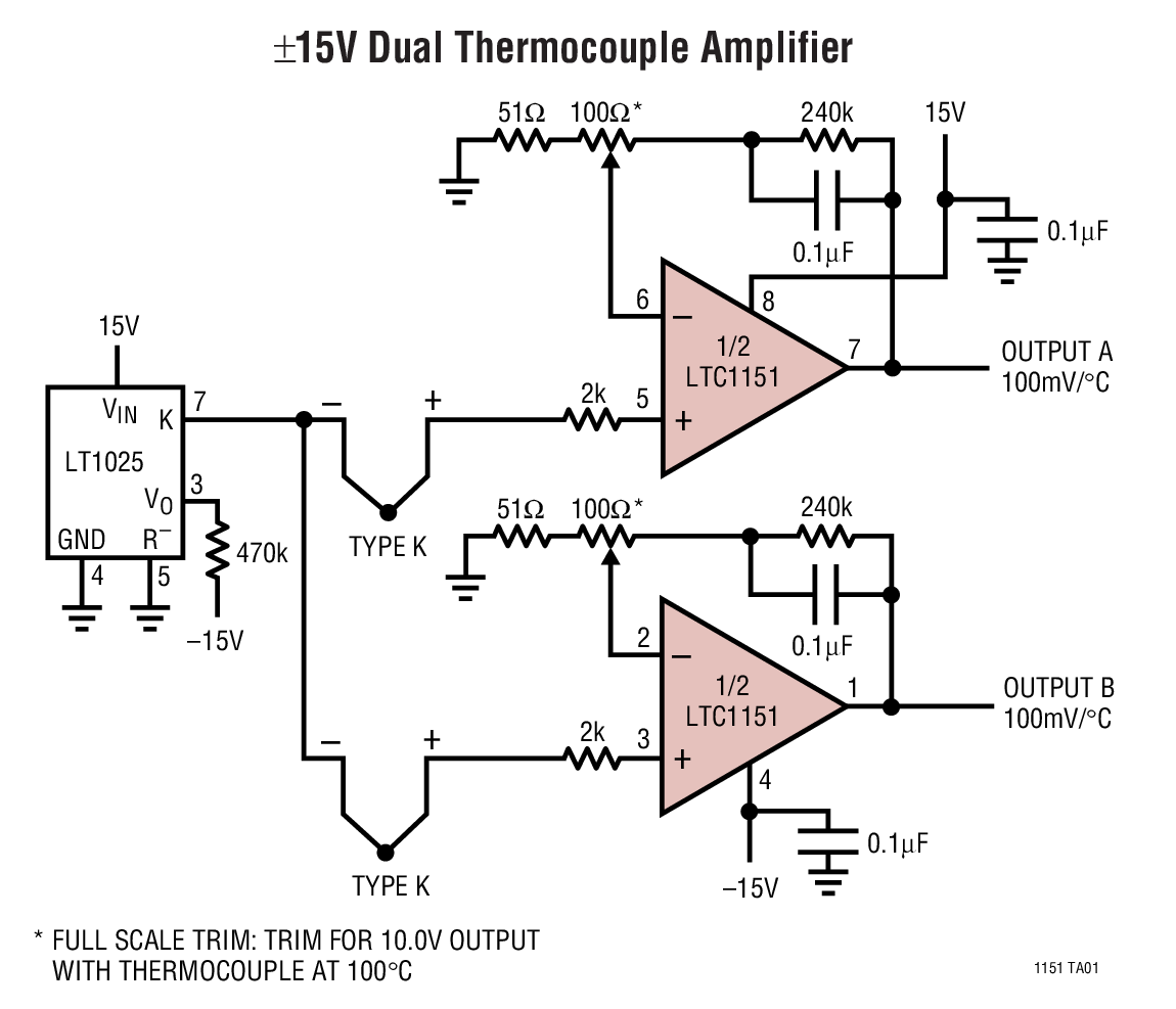
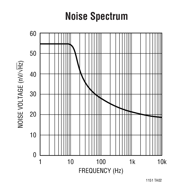
The LTC1151 has a typical offset voltage of 0.5µV, drift of 0.01µV/°C, 0.1Hz to 10Hz input noise voltage of .5mVP-P, and a typical voltage gain of 140dB. It has a slew rate of 3V/µs and a gain-bandwidth product of 2.5MHz with a supply current of 0.9mA per amplifier. Overload recovery times from positive and negative saturation are 3ms and 20ms, respectively.
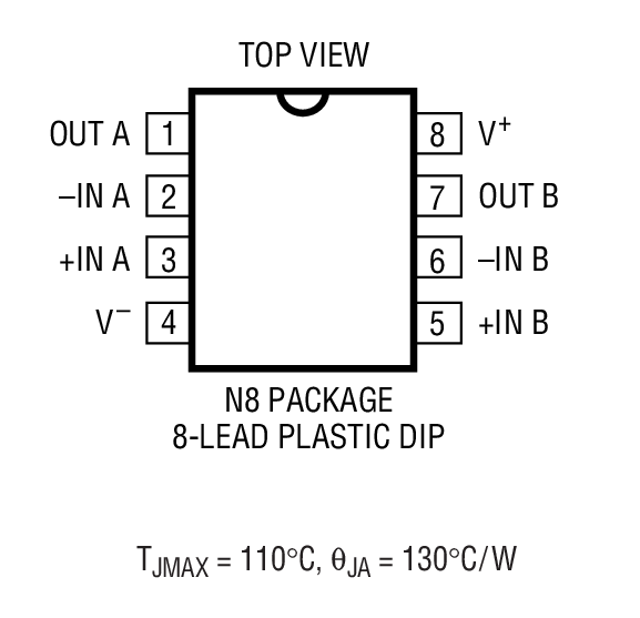
The LTC1151 is available in a standard 8-lead plastic DIP package as well as a 16-lead wide body SO. The LTC1151 is pin compatible with industry-standard dual op amps and runs from standard ±15V supplies, allowing it to plug in to most standard bipolar op amp sockets while offering significant improvement in DC performance.
| 器件型号 | 封装 | 温度 | 价格 (以 1 ~ 99 片为批量) | 价格 (以 1000 片为批量) * |
|---|---|---|---|---|
| LTC1151CN8#PBF | N-8 | C | $7.15 | $5.80 |
| LTC1151CSW#PBF | SW-16 | C | $8.35 | $6.75 |
| LTC1151CSW#TRPBF | SW-16 | C | $6.81 |


