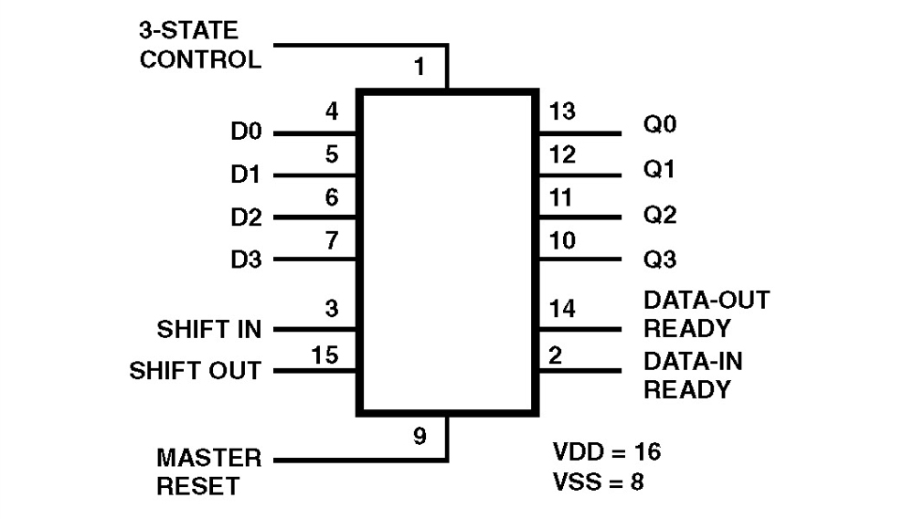
CD40105BMS is a low-power first-in-first-out (FIFO) "elastic" storage register that can store 16 4-bit words. It is capable of handling input and output data at different shifting rates. This feature makes it particularly useful as a buffer between asynchronous systems.
Each word position in the register is clocked by a control flip- flop, which stores a marker bit. A "1" signifies that the position's data is filled and a "0" denotes a vacancy in that position. The control flip-flop detects the state of the preceding flip-flop and communicates its own status to the succeeding flip-flop. When a control flip-flop is in the "0" state and sees a "1" in the preceding flip-flop, it generates a clock pulse that transfers data from the preceding four data latches into its own four data latches and resets the preceding flip-flop to "0". The first and last control flip-flops have buffered outputs. Since all empty locations "bubble" automatically to the input end, and all valid data ripple through to the output end, the status of the first control flip-flop (DATA-IN READY) indicates if the FIFO is full, and the status of the last flip-flop (DATAOUT READY) indicates if the FIFO contains data. As the earliest data are removed from the bottom of the data stack (the output end), all data entered later will automatically propagate (ripple) toward the output.
Key Features
- 4 Bits x 16 Words
- High Voltage Type (20V Rating)
- Independent Asynchronous Inputs and Outputs
- 3-State Outputs
- Expandable in Either Direction
- Status Indicators on Input and Output
- Reset Capability
- Standardized Symmetrical Output Characteristics
- 100% Tested for Quiescent Current at 20V
- 5V, 10V and 15V Parametric Ratings
- Maximum Input Current of 1µA at 18V Over Full Package Temperature Range; 100nA at 18V and +25oC
- Noise Margin (Over Full Package/Temperature Range)
- 1V at VDD = 5V
- 2V at VDD = 10V
- 2.5V at VDD = 15V
- Meets All Requirements of JEDEC Tentative Standard No. 13B, "Standard Specifications for Description of 'B' Series CMOS Devices"
Applications
- Bit Rate Smoothing
- CPU/Terminal Buffering
- Data Communications
- Peripheral Buffering
- Line Printer Input Buffers
- Auto Dialers
- CRT Buffer Memories
- Radar Data Acquisition

Order Information| Part Number | Package Type | Weight(g) | Pins | MSL Rating | Peak Temp (°C) | RoHS Status |
|---|
|
| CD40105BDMSR | 16 Ld SBDIP | 1.37 | 16 | N/A | NA | RoHS |
|
|
| CD40105BKMSR | 16 Ld CFP | 0.59 | 16 | N/A | NA | RoHS |
|
|

