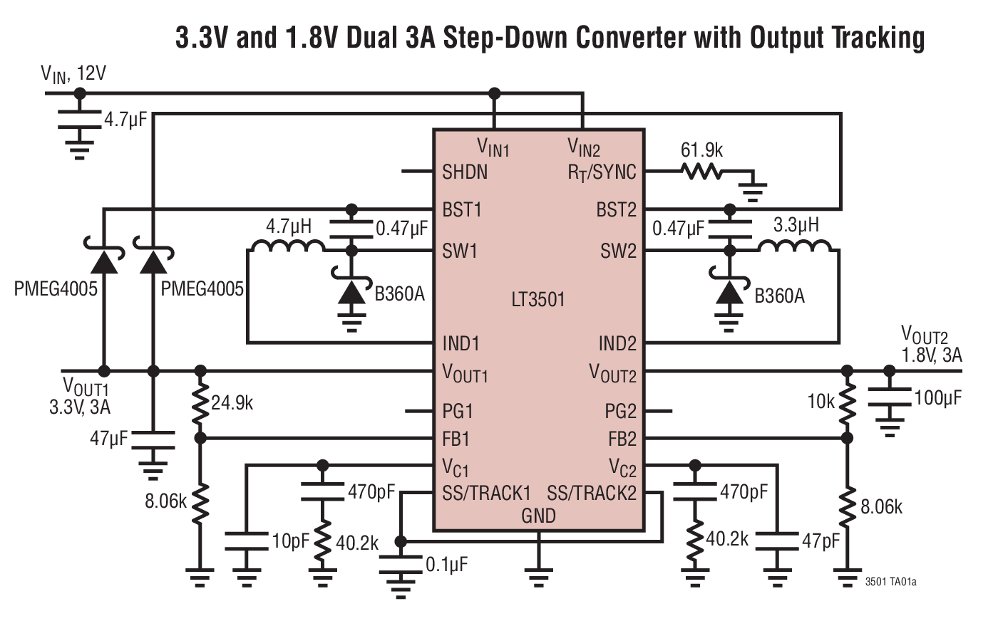
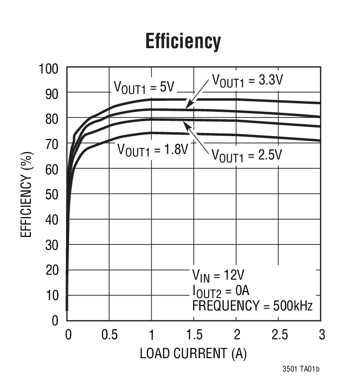
LT3501 - Monolithic Dual Tracking 3A Step-Down Switching Regulator
Both converters are synchronized to either a common external clock input or a resistor programmable fi xed 250kHz to 1.5MHz internal oscillator. At all frequencies, a 180° phase relationship between channels is maintained, reducing voltage ripple and component size. Programmable frequency allows for optimization between effi ciency and external component size.
Minimum input-to-output voltage ratios are improved by allowing the switch to stay on through multiple clock cycles, only switching off when the boost capacitor needs recharging, resulting in ~95% maximum duty cycle.
Each output can be independently disabled using its own soft-start pin, or by using the SHDN pin the entire part can be placed in a low quiescent current shutdown mode.
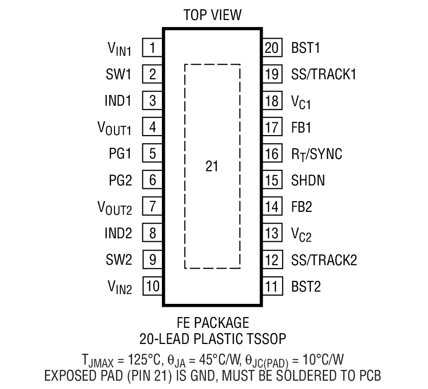
The LT3501 is available in a 20-lead TSSOP package with exposed leadframe for low thermal resistance.
Order Information
| Part Number | Package | Temp | Price(1-99) | Price (1k)* |
|---|---|---|---|---|
| LT3501EFE#PBF | TSSOP-20 | E | $5.41 | $3.50 |
| LT3501EFE#TRPBF | TSSOP-20 | E | $3.55 | |
| LT3501IFE#PBF | TSSOP-20 | I | $6.48 | $4.20 |
| LT3501IFE#TRPBF | TSSOP-20 | I | $4.25 |
Demo Boards
| Part Number | Description | Price |
|---|---|---|
| DC964A | LT3501EFE Demo Board | Dual, 4.5V ≤ VIN ≤ 24V, Vout1 = 3.3V @ 3A, Vout2 = 1.8V @ 3A | $225.00 |


