74LVC595ABQ: 8-bit serial-in/serial-out or parallel-out shift register; 3-state
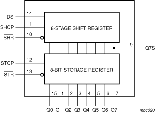
The 74LVC595A is an 8-bit serial-in/serial or parallel-out shift register with a storage register and 3-state outputs. Both the shift and storage register have separate clocks.
The input can be driven from either 3.3 V or 5 V devices. This feature allows the use of this device in a mixed 3.3 V and 5 V environment.
This device is fully specified for partial Power-down applications using IOFF. The IOFF circuitry disables the output, preventing the damaging backflow current through the device when it is powered down.
Data is shifted on the positive-going transitions of the SHCP input. The data in the shift register is transferred to the storage register on a positive-going transition of the STCP input. If both clocks are connected together, the shift register will always be one clock pulse ahead of the storage register.
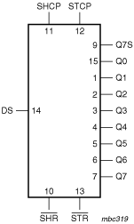
The shift register has a serial input (DS) and a serial output (Q7S) for cascading purposes. It is also provided with asynchronous reset input MR (active LOW) for all 8 shift register stages. The storage register has 8 parallel 3-state bus driver outputs. Data in the storage register appears at the output whenever the output enable input (OE) is LOW.
74LVC595ABQ: Product Block Diagram

74LVC595ABQ: Block Diagram

74LVC595ABQ: Block Diagram

Outline 3d SOT763-1

Data Sheets (1)
| Name/Description | Modified Date |
|---|---|
| 8-bit serial-in/serial-out or parallel-out shift register; 3-state (REV 2.0) PDF (203.0 kB) 74LVC595A [English] | 20 Jun 2014 |
Application Notes (5)
| Name/Description | Modified Date |
|---|---|
| Sorting through the low voltage logic maze (REV 1.0) PDF (72.0 kB) AN10156 [English] | 13 Mar 2013 |
| Package lead inductance considerations in high-speed applications (REV 1.0) PDF (43.0 kB) AN212 [English] | 13 Mar 2013 |
| Pin FMEA for LVC family (REV 1.0) PDF (44.0 kB) AN11009 [English] | 04 Feb 2011 |
| Power considerations when using CMOS and BiCMOS logic devices (REV 1.0) PDF (100.0 kB) AN263 [English] | 05 Feb 2002 |
| Interfacing 3 Volt and 5 Volt Applications (REV 1.0) PDF (63.0 kB) AN240 [English] | 15 Sep 1995 |
Package Information (1)
| Name/Description | Modified Date |
|---|---|
| plastic dual in-line compatible thermal enhanced very thin quad flat package; no leads; 16 terminals; body 2.5 x 3.5 x... (REV 1.1) PDF (191.0 kB) SOT763-1 [English] | 30 May 2016 |
Packing (1)
| Name/Description | Modified Date |
|---|---|
| DHVQFN16; Reel pack, SMD, 7" Q1/T1 standard product orientation Orderable part number ending ,115 or... (REV 2.0) PDF (191.0 kB) SOT763-1_115 [English] | 05 Jul 2016 |
IBIS Model
- 74LVC595A IBIS model (REV 1.0) ibs LVC595A 10/22/2014
Ordering Information
| Product | Status | Family | VCC (V) | Function | Logic switching levels | Description | Output drive capability (mA) | Package version | tpd (ns) | fmax (MHz) | No of bits | Power dissipation considerations | Tamb (Cel) | Rth(j-a) (K/W) | Ψth(j-top) (K/W) | Rth(j-c) (K/W) | Package name | No of pins |
|---|---|---|---|---|---|---|---|---|---|---|---|---|---|---|---|---|---|---|
| 74LVC595ABQ | Active | LVC | 1.2 - 5.5 | Shift registers | CMOS/LVTTL | 8-bit serial-in/parallel-out shift register with output storage register (3-state) | +/- 24 | SOT763-1 | 4 | 180 | 8 | low | -40~125 | 92 | 13.3 | 61 | DHVQFN16 | 16 |
Package Information
| Product ID | Package Description | Outline Version | Reflow/Wave Soldering | Packing | Product Status | Part NumberOrdering code(12NC) | Marking | Chemical Content | RoHS / Pb Free / RHF | LeadFree Conversion Date | EFR | IFR(FIT) | MTBF(hour) | MSL | MSL LF |
|---|---|---|---|---|---|---|---|---|---|---|---|---|---|---|---|
| 74LVC595ABQ |  | SOT763-1 | Reel 7" Q1/T1 | Active | 74LVC595ABQ,115 (9352 824 68115) | VC595A | 74LVC595ABQ |    | Always Pb-free | 123.8 | 3.87 | 2.58E8 | 1 | 1 |
