CBTU4411EE: 11-bit DDR2 SDRAM MUX/bus switch with 12 Ω ON resistance
This 11-bit bus switch is designed for 1.7 V to 1.9 V VDD operation and SSTL_18 select input levels.
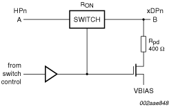
Each Host port pin (HPn) is multiplexed to one of four DIMM port pins (xDPn). The selection of the DIMM port to be connected to the Host port is controlled by a decoder driven by three hardware select pins S0, S1 and EN. Driving pin EN HIGH disconnects all DIMM ports from their respective host ports. When EN is driven LOW, pins S0 and S1 select one of four DIMM ports to be connected to their respective host port. When disconnected, any DIMM port is terminated to the externally supplied voltage Vbias by means of an on-chip pull-down resistor of typically 400 Ω. The ON-state connects the Host port to the DIMM port through a 12 Ω nominal series resistance. The design is intended to have only one DIMM port active at any time.
The CBTU4411 can also be configured to support a differential strobe signal on channel 10 (TRUE) and channel 9 (complementary Strobe). When its LVCMOS configuration input strobe enable (STREN) is HIGH, channel 10 is pulled up to 3/4 of VDD internally by a resistive divider when the DIMM port is idle. When the CBTU4411 is disabled (EN = HIGH in Strobe mode), the pull-down on channel 10 is disabled for current savings, pulling channel 10 to VDD. When strobe enable (STREN) is LOW, channel 10 behaves the same as all other channels.
The select inputs (S0, S1) are pseudo-differential type SSTL_18. A reference voltage should be provided to input pin VREF at nominally 0.5VDD. This topology provides accurate control of switching times by reducing dependency on select signal slew rates. S0 and S1 are provided with selectable input termination to 0.5VDD (active when LVCMOS input TERM is HIGH). When the CBTU4411 is disabled (EN = HIGH), both S0 and S1 inputs are pulled LOW.
The part incorporates a very low crosstalk design. It has a very low skew between outputs (< 30 ps) and low skew (< 30 ps) for rising and falling edges. The part has optimal performance in DDR2 data bus applications.
Each switch has been optimized for connection to 1- or 2-rank DIMMs.
The low internal RC time constant of the switch allows data transfer to be made with minimal propagation delay.
The CBTU4411 is characterized for operation from 0 °C to +85 °C.
CBTU4411EE: Product Block Diagram

CBTU4411EE: Block Diagram

CBTU4411EE: Block Diagram

sot856-1_3d

Data Sheets (1)
| Name/Description | Modified Date |
|---|---|
| 11-bit DDR2 SDRAM MUX/bus switch with 12 Ohm ON resistance (REV 4.0) PDF (173.0 kB) CBTU4411 | 18 Jun 2012 |
Package Information (1)
| Name/Description | Modified Date |
|---|---|
| plastic low profile fine-pitch ball grid array package; 72 balls; body 7 x 7 x 1.05 mm (REV 1.0) PDF (365.0 kB) SOT856-1 | 08 Feb 2016 |
Ordering Information
| Product | Status | Family | Package version | Description | Outputs | Other features | Tamb (Cel) | Operating voltage (VDC) | Package name |
|---|---|---|---|---|---|---|---|---|---|
| CBTU4411EE | Active | SOT856-1 | LFBGA72 | ||||||
| CBTU4411EE/G | No Longer Manufactured | LFBGA72 |
Package Information
| Product ID | Package Description | Outline Version | Reflow/Wave Soldering | Packing | Product Status | Part NumberOrdering code(12NC) | Marking | Chemical Content | RoHS / Pb Free / RHF | LeadFree Conversion Date | MSL | MSL LF |
|---|---|---|---|---|---|---|---|---|---|---|---|---|
| CBTU4411EE |  | SOT856-1 | Reel 13" Q1/T1 in Drypack | Active | CBTU4411EE,518 (9352 769 13518) | CBTU4411EE | CBTU4411EE |    | Always Pb-free | NA | 3 | |
| Tray, Bakeable, Multiple in Drypack | Active | CBTU4411EE,557 (9352 769 13557) | CBTU4411EE | CBTU4411EE |    | Always Pb-free | NA | 3 | ||||
| Tray, Bakeable, Single in Drypack | Active | CBTU4411EE,551 (9352 769 13551) | CBTU4411EE | CBTU4411EE |    | Always Pb-free | NA | 3 |
- plastic low profile fine-pitch ball grid array package; 72 balls; body 7 x 7 x 1.05 mm CBTU4411EE
- CBTU4411EE
- CBTU4411EE
- CBTU4411EE
