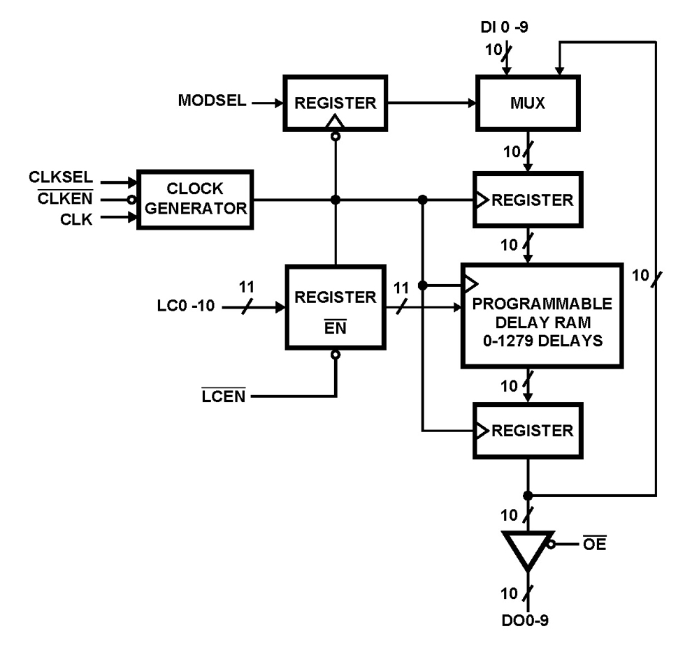
The HSP9501 is a 10-Bit wide programmable data buffer designed for use in high speed digital systems. Two different modes of operation can be selected through the use of the MODSEL input. In the delay mode, a programmable data pipeline is created which can provide 2 to 1281 clock cycles of delay between the input and output data. In the data recirculate mode, the output data path is internally routed back to the input to provide a programmable circular buffer.
The length of the buffer or amount of delay is programmed through the use of the 11-bit Length Control Input Port (LC0-10) and the Length Control Enable (LCEN). An 11-bit value is applied to the LC0-10 inputs, LCEN is asserted, and the next selected clock edge loads the new count value into the Length Control Register. The delay path of the HSP9501 consists of two registers with a programmable delay RAM between them, therefore, the value programmed into the Length Control Register is the desired length - 2. The range of values which can be programmed into the Length Control Register are from 0 to 1279, which in turn results in an overall range of programmable delays from 2 to 1281.
Clock select logic is provided to allow the use of a positive or negative edge system clock as the CLK input to the HSP9501. The active edge of the CLK input is controlled through the use of the CLKSEL input. All synchronous timing (i.e., data setup, hold, and output delays) are relative to the clock edge selected by CLKSEL. An additional clock enable input (CLKEN) provides a means of disabling the internal clock and holding the existing contents temporarily. All outputs of the HSP9501 are three-state outputs to allow direct interfacing to system or multi-use buses.
The HSP9501 is recommended for digital video processing or any applications which require a programmable delay or circular data buffer.
Key Features
- DC to 32MHz Operating Frequency
- Programmable Buffer Length from 2 to 1281 Words
- Supports Data Words to 10 Bits
- Clock Select Logic for Positive or Negative Edge System Clocks
- Data Recirculate or Delay Modes of Operation
- Expandable Data Word Width or Buffer Length
- Three-State Outputs
- TTL Compatible Inputs/Outputs
- Low Power CMOS
Applications
- Sample Rate Conversion
- Data Time Compression/Expansion
- Software Controlled Data Alignment
- Programmable Serial Data Shifting
- Audio/Speech Data Processing Video/Image Processing

Order Information| Part Number | Package Type | Weight(g) | Pins | MSL Rating | Peak Temp (°C) | RoHS Status |
|---|
|
| HSP9501JC-25 | 44 Ld PLCC | 2.31 | 44 | 4 | 225 | |
|
|
| HSP9501JC-32 | 44 Ld PLCC | 2.31 | 44 | 4 | 225 | |
|
|


