HMC842LC4B 45 Gbps Fanout Buffer with Programmable Output Voltage
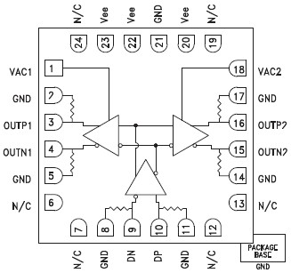
The HMC842LC4B is a 1:2 Fanout Buffer designed to support data transmission rates up to 45 Gbps. The device can also operate with clock signals up to 28 GHz. During normal operation, input data (or clock) is transferred to both output channels. Differential input and output signals of the HMC842LC4B are terminated with 50 Ohms to ground on-chip, and may be either AC or DC coupled. The Outputs can be connected directly to a 50 Ohms-to-ground terminated system, while DC blocking capacitors should be used if the terminating system is 50 Ohms to a non-ground DC voltage. The HMC842LC4B also features two separate output level control pins, VAC1 and VAC2 which provide loss compensation and signal level optimization for each output channel independently. The HMC842LC4B operates from a single -3.3V DC supply and is available in a ceramic RoHS compliant 4x4 mm SMT package
技术特性
- Supports Clock Frequencies
up to 28 GHz
- Independent Programmable
Output Swing for
Each Channel: 400 - 1200 mVp-p Diff.
- Single-Ended or Differential Operation
- Power Consumption: 465 mW
- Less than 500 fs Additive RMS Jitter
- Fast Rise and Fall Times: <12 ps
- 24 Lead 4x4mm SMT Package: 16mm²
订购信息 Ordering Information
应用领域 APPLICATION
-
OC-768 & SDH STM-256 Equipment
-
RF ATE Applications
-
Short, intermediate, & Long Haul
Fiber Optic Applications
-
Broadband Test & Measurement
-
Serial Data Transmission
up to 45 Gbps
-
Clock Buffering up to 28 GHz
|
技术指标
Data/
Clock Rate (Gbps/GHz) |
Function |
Rise/Fall Time
(ps) |
Diff. Output Swing (Vp-p) |
DC Power Consumption (mW) |
DC Power Supply (Vdc) |
Package |
| 45 / 28 |
1:2 Fanout Buffer w/ Adj. Vout |
11 / 11 |
0.4 - 1.2 |
465 |
-3.3 |
LC4B |
功能框图 Functional Block Diagram
|
