HMC843LC4B 45 Gbps Fast Rise Time AND/NAND / OR/NOR wwith Programmable Output
The HMC843LC4B is an AND/NAND/OR/NOR function designed to support data transmission rates of up to 45 Gbps, and clock frequencies as high as 25 GHz. The HMC843LC4B may be easily confi gured to provide any of the following logic functions: AND, NAND, OR and NOR. The HMC843LC4B also features an output level control pin, VAC, which allows for loss compensation or for signal level optimization. All input signals to the HMC843LC4B are terminated with 50 Ohms to ground on-chip, and may be either AC or DC coupled. The differential outputs of the HMC843LC4B may be either AC or DC coupled. Outputs can be connected directly to a 50 Ohms-to-ground terminated system, while DC blocking capacitors should be used if the terminating system is 50 Ohms to a non-ground DC voltage. The HMC843LC4B operates from a single -3.3V DC supply, and is available in a ceramic RoHS compliant 4x4 mm SMT package.
技术特性
- Supports High Data Rates:
up to 45 Gbps
- Differential & Single-Ended Operation
- Fast Rise & Fall Times: 10 / 10 ps
- Low Power Consumption: 530 mW
- Programmable Differential
Output Voltage Swing: 200 - 900 mV
- Single Supply: -3.3V
- 24 Lead Ceramic 4x4mm
SMT Package: 16mm²
订购信息 Ordering Information
应用领域 APPLICATION
- RF ATE Applications
- Broadband Test & Measurement
- Serial Data Transmission
up to 45 Gbps
- Digital Logic Systems up to 25 GHz
- NRZ-to-RZ Conversion
|
技术指标
Data/
Clock Rate (Gbps/GHz) |
Function |
Rise/Fall Time
(ps) |
Diff. Output Swing (Vp-p) |
DC Power Consumption (mW) |
DC Power Supply (Vdc) |
Package |
| 45 / 25 |
AND/NAND/OR/NOR w/ Adj. Vout |
10 / 10 |
0.2 - 0.9 |
530 |
-3.3 |
LC4B |
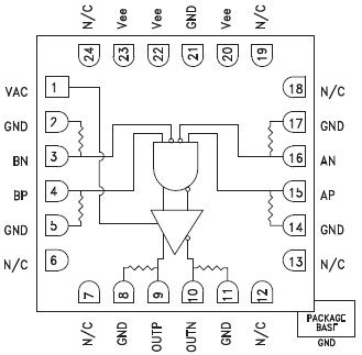
功能框图 Functional Block Diagram
|
