HMC847LC5 45 Gbps, 4:1 Mux SMT with Duty Cycle Control & Programmable Output
The HMC847LC5 is a 4:1 multiplexer designed for 45 Gbps data serialization. The mux latches the four differential inputs on the transition points of the input clock. The device uses both rising and falling edges of the half-rate clock to serialize the data. A quarter-rate clock output, which is synchronous to the data output of HMC847LC5, is generated on chip. All clock and data inputs / outputs of the HMC847LC5 are CML and terminated on-chip with 50 Ohms to the, VCC, and may be DC or AC coupled. The inputs and outputs of the HMC847LC5 may be operated either differentially or single-ended. The HMC847LC5 also features an output level control pin, VCTRL, which allows for loss compensation or signal level optimization. The VDCC pin controls the data output cross-point & duty cycle. The HMC847LC5 operates from a single +3.3V supply and is available in ROHS compliant 5x5 mm SMT package.
技术特性
- Supports Data Rates up to 45 Gbps
- Half Rate Clock Input
- Quarter Rate Reference Clock Output
- Fast Rise and Fall Times: 11 / 12 ps
- Programmable Differential Output
Voltage Swing: 250 - 900 mVp-p
- Single Supply: +3.3V
- 32 Lead 5x5mm SMT Package: 25mm²
订购信息 Ordering Information
应用领域 APPLICATION
- SONET OC-768
- RF ATE Applications
- Broadband Test & Measurement
- Serial Data Transmission
up to 45 Gbps
- High Speed DAC Interfacing
|
技术指标
Data/
Clock Rate (Gbps/GHz) |
Function |
Rise/Fall Time
(ps) |
Diff. Output Swing (Vp-p) |
DC Power Consumption (mW) |
DC Power Supply (Vdc) |
Package |
| 45 / 22.5 |
4:1 Mux with Adj. Vout |
11 / 12 |
0.25 - 0.9 |
1782 |
+3.3 |
LC5 |
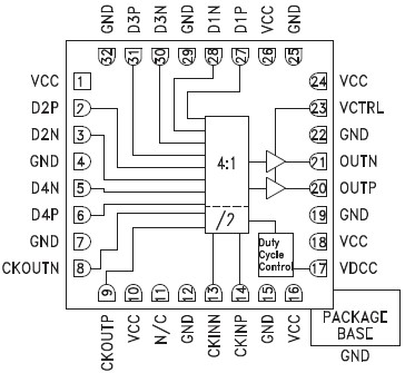
功能框图 Functional Block Diagram
|
