HMC859LC3 26 GHz, Divide-By-8 SMT with Reset & Programmable Output Voltage
The HMC859LC3 is a Divide-by-8 with Reset designed to support clock frequencies as high as 26 GHz. During normal operation, with the reset pin not asserted, the output toggles from its prior state on the positive edge of the clock. Asserting the reset pin forces the Q output low regardless of the clock edge state (asynchronous reset assertion). Reversing the clock inputs allows for negative-edge triggered applications. The HMC859LC3 also features an output level control pin, VR, which allows for loss compensation or for signal level optimization. All input signals to the HMC859LC3 are terminated with 50 Ω to ground on-chip, and may be either AC or DC coupled. Outputs can be connected directly to a 50 Ω terminated system, while DC blocking capacitors may be used if the terminating system is 50 Ω to a non-ground DC voltage. The HMC859LC3 operates from a single -3.3 V DC supply and is available in a ceramic RoHS compliant 3x3 mm SMT package.
技术特性
- Differential & Singe-Ended Operation
- Fast Rise and Fall Times: 19 / 17 ps
- Low Power Consumption: 320 mW typ.
- Programmable Differential Output
Voltage Swing: 800 - 1900 mVp-p
- Propagation Delay: 146 ps
- Single Supply: -3.3V
- 16 Lead 3x3mm SMT Package: 9mm²
订购信息 Ordering Information
应用领域 APPLICATION
- High Speed Frequency Divider
(up to 26 GHz)
- Clock Synthesis
- Phase Locked Loops
- Broadband Test & Measurement
|
技术指标
Data/
Clock Rate (Gbps/GHz) |
Function |
Rise/Fall Time
(ps) |
Diff. Output Swing (Vp-p) |
DC Power Consumption (mW) |
DC Power Supply (Vdc) |
Package |
| - / 26 |
Clock Divide-by-8 |
19 / 17 |
0.8 - 1.8 |
320 |
-3.3 |
LC3 |
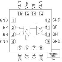
功能框图 Functional Block Diagram
|
