MADP-064908-131000 Surmount TM PIN Chip RoHS Compliant
This device is a silicon glass PIN diode chip fabricated with M/A-COM Tech Solutions patented HMIC process. This 80μm I-region length device features six silicon pedestals embedded in a low loss, low dispersion glass. The diodes are formed on the top of a pedestal and connections to the backside of the device are facilitated by making the pedestal sidewalls electrically conductive. Selective backside metallization is applied producing a surface mount device. The topside is fully encapsulated with silicon nitride and has an additional polymer layer for scratch protection. These protective coatings prevent damage to the junction and the anode air-bridge during handling and assembly. The vertical silicon diode topology provides for a highly efficient heat transfer medium. These surface mount devices are suitable for usage in higher (3W avg.) incident power switches. Small parasitic inductance and excellent RC constant make these devices ideal for absorptive SPST, reflective SP2T switches, and attenuator circuits, where higher P1db and power handling values are required.
技术特性 Features
应用领域ApplicationsThese packageless devices are suitable for moderate incident power applications, ≤ 10W/C.W. or where the peak power is ≤ 52W, pulse width is ≤ 1μS, and duty cycle is ≤ 0.01%. Their low parasitic inductance, 0.4 nH, and excellent RC constant, make these devices a superior choice for higher frequency switch elements when compared to their plastic package counterparts. 订购信息Ordering Information
|
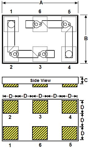
功能框图 Functional Block Diagram
|
| 应用技术支持与电子电路设计开发资源下载 | 版本信息 | 大小 |
|---|---|---|
| MADP-064908-131000 数据资料DataSheet下载.pdf | Rev.V2 | 2 页 |
