AAT3190 Positive/Negative Charge Pump for Voltage Bias
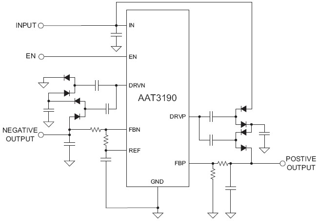
The AAT3190 charge pump controller provides the regulated positive and negative voltage biases required by active matrix thin-film transistor (TFT) liquid-crystal displays (LCDs), charge-coupled device (CCD) sensors, and organic light emitting diodes (OLEDs). Two low-power charge pumps convert input supply voltages ranging from 2.7V to 5.5V into two independent output voltages. The dual low-power charge pumps independently regulate a positive (VPOS) and negative (VNEG) output voltage. These outputs use external diode and capacitor multiplier stages (as many stages as required) to regulate output voltages up to ±25V. Built-in soft-start circuitry prevents excessive in-rush current during start-up. A high switching frequency enables the use of small external capacitors. The device’s shutdown feature disconnects the load from VIN and reduces quiescent current to less than 1.0μA. The AAT3190 is available in a Pb-free MSOP-8 or TSOPJW-12 package and is specified over the -40°C to +85°C operating temperature range.
技术特性
|
应用领域 APPLICATION
订购信息 Ordering Information
AAT3190 典型应用
|
| 应用技术支持与电子电路设计开发资源下载 | 版本信息 | 大小 |
| AAT3190 数据资料DataSheet下载:pdf | Rev.V2 | 2 页 |
