AAT4712 Power Path with Input Current Limit and Capacitor Charger
The AAT4712 is a programmed, current limited P-channel MOSFET power switch designed for high-side load-switching applications for SSD memory buffer saving solutions. With the programmed current limit, the AAT4712 ensures that the power ratings of the host are not exceeded and balances the system load and supercap charging current automatically to provide enough system load current in top-priority. The integrated discharge path control assures that the system load can still be supported in the short term when the input power has not fully charged the supercap. The current limit is programmed by an external resistor allowing ±10% accuracy at room temperature. The AAT4712 integrates discharge path for SYS (to system load) from VCC input or OUT input (connect to supercap). The low RDS(ON) from OUT to SYS prolongs the supercap backup time when VCC drops below a threshold voltage which is programmed by an external resistor from ADJ to ground. The AAT4712 incorporates a POK function which can indicate system input power good. An ADJ pin is provided with the addition of an external resistor for setting the input power good detect threshold. The AAT4712 also incorporates a supercap charge ready (RDY) indicate function. The quiescent supply current is typically a low 70μA from the discharge path of VCC to SYS. The AAT4712 is available in a 16-pin TDFN34 package and is specified over a -40 to 85°C temperature range.
技术特性
|
订购信息 Ordering Information
应用领域 APPLICATION
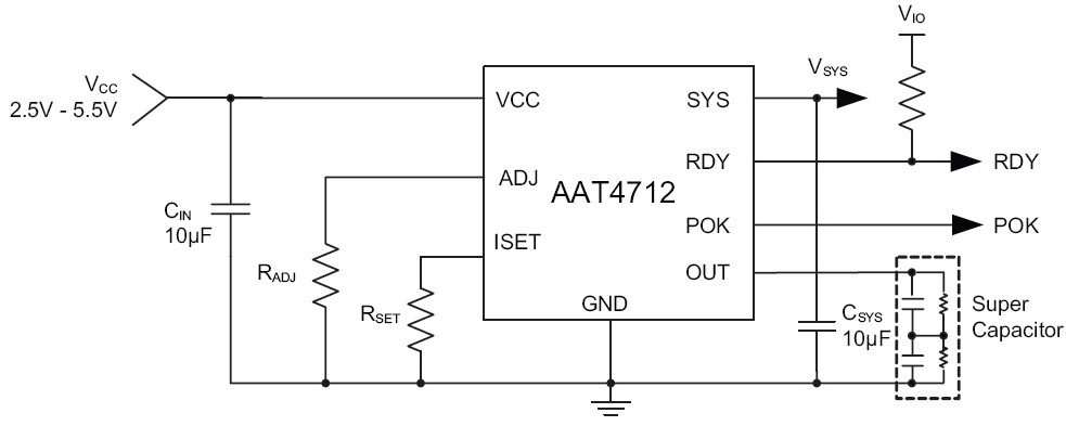
功能框图 Functional Block Diagram
|
| 应用技术支持与电子电路设计开发资源下载 | 版本信息 | 大小 |
| AAT4712 数据资料DataSheet下载:pdf | Rev.V2 | 2 页 |
