SKY77350-13 Power Amplifier Module for quad-band
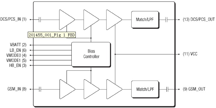
The SKY77350-13 Power Amplifier Module (PAM) is designed in a low profile (0.9 mm), compact form factor for quad-band cellular handsets comprising GSM850/900, DCS1800, and PCS1900 operation. The PAM also supports Class 12 General Packet Radio Service (GPRS) multi-slot operation. The module consists of separate GSM PA and DCS1800/PCS1900 PA blocks, impedance-matching circuitry for 50 input and output impedances and a Power Amplifier Control (PAC) block with an internal current-sense resistor. The custom BiCMOS integrated circuit provides the internal PAC function and interface circuitry. Fabricated onto a single Gallium Arsenide (GaAs) die, one Heterojunction Bipolar Transistor (HBT) PA block supports the GSM bands and the other supports the DCS1800 and PCS1900 bands. Both PA blocks share common power supply pads to distribute current. The GaAs die, the Silicon (Si) die, and the passive components are mounted on a multi-layer laminate substrate. The assembly is encapsulated with plastic overmold. RF input and output ports of the SKY77350-13 are internally matched to a 50 load to reduce the number of external components for a quad-band design. Extremely low leakage current (2.5 A, typical) of the dual PA module maximizes handset standby time. The SKY77350-13 also contains bandselect switching circuitry to select GSM (logic 0) or DCS/PCS (logic 1) as determined from the Band Select (BS) signal. As shown in Figure 1 below, the BS pad selects between the GSM RF input and output pads versus the DCS/PCS RF input and output pads while the Analog Power Control (VRAMP) controls the output power level. The VCC pad connects to an internal current-sense resistor and interfaces to an integrated power amplifier control (iPAC™) function, which is insensitive to variations in temperature, power supply, process, and input power. The BiCMOS controller will shutdown the PA when VCC is raised above the specified operating voltage. The SKY77350-13 is compatible with logic levels from 1.2 V to VCC for BS and ENABLE pads, depending on the level applied to the VLOGIC pad. This feature provides additional flexibility for the designer in the selection of FEM interface control logic.
技术特性
订购信息 Ordering Information
|
应用领域 APPLICATION
功能框图 Functional Block Diagram
|
| 应用技术支持与电子电路设计开发资源下载 | 版本信息 | 大小 |
| SKY77350-13 数据资料DataSheet下载:pdf | Rev.V2 | 2 页 |
