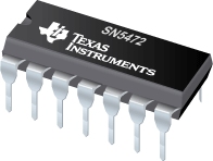
SN5472 具有预设和清零功能的与闸控 J-K 主从触发器
 These J-K flip-flops are based on the master-slave principle and each has AND gate inputs for entry into the master section which are controlled by the clock pulse. The clock pulse also regulates the state of the coupling transistors which connect the master and slave sections. The sequence of operation is as follows:
- 1. Isolate slave from master
- 2. Enter information from AND gate inputs to master
- 3. Disable AND gate inputs
- 4. Transfer information from master to slave
The logical states of the J and K inputs must not be allowed to change when the clock pulse is in a high state.
The SN5472, and the SN54H72 are characterized for operation over the full military temperature range of -55°C to 125°C
| SN5472 | |
| Voltage Nodes(V) | 5 |
| Vcc range(V) | 4.5 to 5.5 |
| Input Level | TTL |
| Output Level | TTL |
| Output | 2S |
| No. of Bits | 1 |
| Technology Family | TTL |
| Rating | Military |
SN5472 特性
- Packages Options Include Plastic and Ceramic DIPs and Ceramic Flat Packages
- Dependable Texas Instruments Quality and Reliability
SN5472 芯片订购指南
| 器件 | 状态 | 温度 | 价格(美元) | 封装 | 引脚 | 封装数量 | 封装载体 | 丝印标记 |
| SN5472J | ACTIVE | -55 to 125 | 4.24 | 1ku | CDIP (J) | 14 | 1 | TUBE |
SN5472 质量与无铅数据
| 器件 | 环保计划* | 铅/焊球涂层 | MSL 等级/回流焊峰 | 环保信息与无铅 (Pb-free) | DPPM / MTBF / FIT 率 |
| SN5472J | TBD | A42 | N/A for Pkg Type | SN5472J | SN5472J |
SN5472 应用技术支持与电子电路设计开发资源下载
- SN5472 数据资料 dataSheet 下载.PDF
- TI 德州仪器触发器/锁存器/寄存器产品选型与价格 . xls
- Shelf-Life Evaluation of Lead-Free Component Finishes (PDF 1305 KB)
- Understanding and Interpreting Standard-Logic Data Sheets (PDF 857 KB)
- TI IBIS File Creation, Validation, and Distribution Processes (PDF 380 KB)
- Implications of Slow or Floating CMOS Inputs (PDF 101 KB)
- CMOS Power Consumption and CPD Calculation (PDF 89 KB)
- Designing With Logic (PDF 186 KB)
- Live Insertion (PDF 150 KB)
- Input and Output Characteristics of Digital Integrated Circuits (PDF 1708 KB)
- Using High Speed CMOS and Advanced CMOS in Systems With Multiple Vcc (PDF 43 KB)
- HiRel Unitrode Power Management Brochure (PDF 206 KB)
- LOGIC Pocket Data Book (PDF 6001 KB)
- HiRel Unitrode Power Management Brochure (PDF 206 KB)
- Logic Cross-Reference (PDF 2938 KB)
