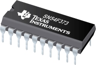
SN54F373 具有三态输出的八路透明 D 类锁存器
 These 8-bit latches feature 3-state outputs designed specifically for driving highly capacitive or relatively low-impedance loads. They are particularly suitable for implementing buffer registers, I/O ports, bidirectional bus drivers, and working registers.
The eight latches of the ´F373 are transparent D-type latches. While the latch-enable (LE) input is high, the Q outputs will follow the data (D) inputs. When the latch enable is taken low, the Q outputs are latched at the logic levels set up at the D inputs.
A buffered output-enable (![]() ) input can be used to place the eight outputs in either a normal
logic state (high or low logic levels) or a high-impedance state. In the high-impedance state, the outputs neither load nor drive the bus lines significantly
) input can be used to place the eight outputs in either a normal
logic state (high or low logic levels) or a high-impedance state. In the high-impedance state, the outputs neither load nor drive the bus lines significantly
| SN54F373 | |
| Voltage Nodes(V) | 5 |
| Rating | Military |
SN54F373 特性
- Eight Latches in a Single Package
- 3-State Bus-Driving True Outputs
- Full Parallel Access for Loading
- Buffered Control Inputs
- Package Options Include Plastic Small-Outline (SOIC) and Shrink Small-Outline (SSOP) Packages, Ceramic Chip Carriers, and Plastic and Ceramic DIPs
SN54F373 芯片订购指南
| 器件 | 状态 | 温度 | 价格(美元) | 封装 | 引脚 | 封装数量 | 封装载体 | 丝印标记 |
| SN54F373FK | ACTIVE | 5962-9074601M2A | 19.16 | 1ku | LCCC (FK) | 20 | 1 | TUBE | |
| SN54F373J | ACTIVE | 5962-9074601MRA | 12.02 | 1ku | CDIP (J) | 20 | 1 | TUBE | |
| SN54F373W | ACTIVE | 5962-9074601MSA | 13.44 | 1ku | CFP (W) | 20 | 1 | TUBE |
SN54F373 质量与无铅数据
| 器件 | 环保计划* | 铅/焊球涂层 | MSL 等级/回流焊峰 | 环保信息与无铅 (Pb-free) | DPPM / MTBF / FIT 率 |
| SN54F373FK | TBD | POST-PLATE | N/A for Pkg Type | SN54F373FK | SN54F373FK |
| SN54F373J | TBD | A42 | N/A for Pkg Type | SN54F373J | SN54F373J |
| SN54F373W | TBD | Call TI | N/A for Pkg Type | SN54F373W | SN54F373W |
SN54F373 应用技术支持与电子电路设计开发资源下载
- SN54F373 数据资料 dataSheet 下载.PDF
- TI 德州仪器触发器/锁存器/寄存器产品选型与价格 . xls
- Shelf-Life Evaluation of Lead-Free Component Finishes (PDF 1305 KB)
- Understanding and Interpreting Standard-Logic Data Sheets (PDF 857 KB)
- TI IBIS File Creation, Validation, and Distribution Processes (PDF 380 KB)
- Implications of Slow or Floating CMOS Inputs (PDF 101 KB)
- CMOS Power Consumption and CPD Calculation (PDF 89 KB)
- Designing With Logic (PDF 186 KB)
- Live Insertion (PDF 150 KB)
- Input and Output Characteristics of Digital Integrated Circuits (PDF 1708 KB)
- Using High Speed CMOS and Advanced CMOS in Systems With Multiple Vcc (PDF 43 KB)
- HiRel Unitrode Power Management Brochure (PDF 206 KB)
- LOGIC Pocket Data Book (PDF 6001 KB)
- HiRel Unitrode Power Management Brochure (PDF 206 KB)
- Logic Cross-Reference (PDF 2938 KB)
