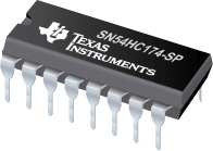
SN54HC174-SP 具有清零功能的六路 D 类触发器
 These positive-edge-triggered D-type flip-flops have a direct clear (CLR)\ input.
Information at the data (D) inputs meeting the setup time requirements is transferred to the outputs on the positive-going edge of the clock (CLK) pulse. Clock triggering occurs at a particular voltage level and is not directly related to the transition time of the positive-going edge of CLK. When CLK is at either the high or low level, the D input has no effect at the output
| SN54HC174-SP | |
| Voltage Nodes(V) | 5 |
| Rating | Military |
SN54HC174-SP 特性
- Wide Operating Voltage Range of 2 V to 6 V
- Outputs Can Drive Up To 10 LSTTL Loads
- Low Power Consumption, 80-µA Max ICC
- Typical tpd = 14 ns
- ±4-mA Output Drive at 5 V
- Low Input Current of 1 µA Max
- Contain Six Flip-Flops With Single-Rail Outputs
- Applications Include:
- Buffer/Storage Registers
- Shift Registers
- Pattern Generators
SN54HC174-SP 芯片订购指南
| 器件 | 状态 | 温度 | 价格(美元) | 封装 | 引脚 | 封装数量 | 封装载体 | 丝印标记 |
| SN54HC174-SPJ | ACTIVE | -55 to 125 | 4.24 | 1ku | CDIP (J) | 16 | 1 | TUBE |
SN54HC174-SP 质量与无铅数据
| 器件 | 环保计划* | 铅/焊球涂层 | MSL 等级/回流焊峰 | 环保信息与无铅 (Pb-free) | DPPM / MTBF / FIT 率 |
| SN54HC174-SPJ | TBD | A42 | N/A for Pkg Type | SN54HC174-SPJ | SN54HC174-SPJ |
SN54HC174-SP 应用技术支持与电子电路设计开发资源下载
- SN54HC174-SP 数据资料 dataSheet 下载.PDF
- TI 德州仪器触发器/锁存器/寄存器产品选型与价格 . xls
- Shelf-Life Evaluation of Lead-Free Component Finishes (PDF 1305 KB)
- Understanding and Interpreting Standard-Logic Data Sheets (PDF 857 KB)
- TI IBIS File Creation, Validation, and Distribution Processes (PDF 380 KB)
- Implications of Slow or Floating CMOS Inputs (PDF 101 KB)
- CMOS Power Consumption and CPD Calculation (PDF 89 KB)
- Designing With Logic (PDF 186 KB)
- Live Insertion (PDF 150 KB)
- Input and Output Characteristics of Digital Integrated Circuits (PDF 1708 KB)
- Using High Speed CMOS and Advanced CMOS in Systems With Multiple Vcc (PDF 43 KB)
- HiRel Unitrode Power Management Brochure (PDF 206 KB)
- LOGIC Pocket Data Book (PDF 6001 KB)
- HiRel Unitrode Power Management Brochure (PDF 206 KB)
- Logic Cross-Reference (PDF 2938 KB)
