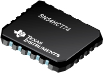
SN54HCT74 具有清零和预设功能的双路 D 类上升沿触发器

The ’HCT74 devices contain two independent D-type positive-edge-triggered flip-flops. A low level at the preset (PRE)\ or clear (CLR)\ inputs sets or resets the outputs, regardless of the levels of the other inputs. When PRE\ and CLR\ are inactive (high), data at the data (D) input meeting the setup time requirements are transferred to the outputs on the positive-going edge of the clock (CLK) pulse. Clock triggering occurs at a voltage level and is not directly related to the rise time of CLK. Following the hold-time interval, data at the D input may be changed without affecting the levels at the outputs.
| SN54HCT74 | |
| Voltage Nodes (V) | 5 |
| Vcc range (V) | 4.5 to 5.5 |
| Input Level | TTL |
| Output Level | CMOS |
| Output | 3S |
| No. of Bits | 2 |
| Technology Family | HCT |
| Rating | Military |
SN54HCT74 特性
- Operating Voltage Range of 4.5 V to 5.5 V
- Outputs Can Drive Up To 10 LSTTL Loads
- Low Power Consumption, 40-µA Max ICC
- Typical tpd = 17 ns
- ±4-mA Output Drive at 5 V
- Low Input Current of 1 µA Max
- Inputs Are TTL-Voltage Compatible
SN54HCT74 芯片订购指南
| 器件 | 状态 | 温度 | 价格(美元) | 封装 | 引脚 | 封装数量 | 封装载体 | 丝印标记 |
| JM38510/65352B2A | ACTIVE | -55 to 125 | 17.93 | 1ku | LCCC (FK) | 20 | 1 | TUBE | |
| JM38510/65352BCA | ACTIVE | -55 to 125 | 16.01 | 1ku | CDIP (J) | 14 | 1 | TUBE | |
| JM38510/65352BDA | ACTIVE | -55 to 125 | 15.25 | 1ku | CFP (W) | 14 | 1 | TUBE | |
| M38510/65352B2A | ACTIVE | -55 to 125 | 17.93 | 1ku | LCCC (FK) | 20 | 1 | TUBE | |
| M38510/65352BCA | ACTIVE | -55 to 125 | 16.01 | 1ku | CDIP (J) | 14 | 1 | TUBE | |
| M38510/65352BDA | ACTIVE | -55 to 125 | 15.25 | 1ku | CFP (W) | 14 | 1 | TUBE |
SN54HCT74 应用手册
SN54HCT74 质量与无铅数据
| 器件 | 环保计划* | 铅/焊球涂层 | MSL 等级/回流焊峰 | 环保信息与无铅 (Pb-free) | DPPM / MTBF / FIT 率 |
| JM38510/65352B2A | TBD | POST-PLATE | N/A for Pkg Type | JM38510/65352B2A | JM38510/65352B2A |
| JM38510/65352BCA | TBD | A42 | N/A for Pkg Type | JM38510/65352BCA | JM38510/65352BCA |
| JM38510/65352BDA | TBD | A42 | N/A for Pkg Type | JM38510/65352BDA | JM38510/65352BDA |
| M38510/65352B2A | TBD | POST-PLATE | N/A for Pkg Type | M38510/65352B2A | M38510/65352B2A |
| M38510/65352BCA | TBD | A42 | N/A for Pkg Type | M38510/65352BCA | M38510/65352BCA |
| M38510/65352BDA | TBD | A42 | N/A for Pkg Type | M38510/65352BDA | M38510/65352BDA |
SN54HCT74 应用技术支持与电子电路设计开发资源下载
- SN54HCT74 数据资料 dataSheet 下载.PDF
- TI 德州仪器触发器/锁存器/寄存器产品选型与价格 . xls
- (选择指南)逻辑器件指南 2009 (Rev. Z)
- (选择指南)小尺寸逻辑器件指南 (Rev. D)
- (用户指南)LOGIC Pocket Data Book
- (用户指南)Signal Switch Data Book
- (用户指南)LVC and LV Low-Voltage CMOS Logic Data Book
- 2008年第一季度通信基础设施方案指南 (Rev. G)
- Communications Infrastructure Solutions Guide 1Q2010
- Design Summary for WCSP Little Logic
- Standard Linear & Logic for PCs, Servers & Motherboards
- STANDARD LINEAR AND LOGIC FOR DVD/VCD PLAYERS
- Military Low Voltage Solutions
- Low-Voltage Logic (LVC) Designer's Guide
- Logic Cross-Reference
