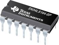
SN54LS164-SP 8 位并行输出串行移位寄存器
 These 8-bit shift registers feature gated serial inputs and an asynchronous clear. The gated serial inputs (A and B) permit complete control over incoming data as a low at either input inhibits entry of the new data and resets the first flip-flop to the low level at the next clock pulse. A high-level input enables the other input which will then determine the state of the first flip-flop. Data at the serial inputs may be changed while the clock is high or low, but only information meeting the setup-time requirements will be entered. Clocking occurs on the low-to-high-level transition of the clock input. All inputs are diode-clamped to minimize transmission-line effects.
The SN54164 and SN54LS164 are characterized for operation over the full military temperature range of -55°C to 125°
| SN54LS164-SP | |
| Technology Family | LS |
| Rating | Space |
SN54LS164-SP 特性
- Gated Serial Inputs
- Fully Buffered Clock and Serial Inputs
- Asynchronous Clear
SN54LS164-SP 应用技术支持与电子电路设计开发资源下载
- SN54LS164-SP 数据资料 dataSheet 下载.PDF
- TI 德州仪器触发器/锁存器/寄存器产品选型与价格 . xls
- Shelf-Life Evaluation of Lead-Free Component Finishes (PDF 1305 KB)
- Understanding and Interpreting Standard-Logic Data Sheets (PDF 857 KB)
- TI IBIS File Creation, Validation, and Distribution Processes (PDF 380 KB)
- Implications of Slow or Floating CMOS Inputs (PDF 101 KB)
- CMOS Power Consumption and CPD Calculation (PDF 89 KB)
- Designing With Logic (PDF 186 KB)
- Live Insertion (PDF 150 KB)
- Input and Output Characteristics of Digital Integrated Circuits (PDF 1708 KB)
- Using High Speed CMOS and Advanced CMOS in Systems With Multiple Vcc (PDF 43 KB)
- HiRel Unitrode Power Management Brochure (PDF 206 KB)
- LOGIC Pocket Data Book (PDF 6001 KB)
- HiRel Unitrode Power Management Brochure (PDF 206 KB)
- Logic Cross-Reference (PDF 2938 KB)
