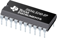
SN54LS240-SP 具有三态输出的八路缓冲器和线路驱动器

These octal buffers and line drivers are designed specifically to improve both the performance and density of three-state memory address drivers, clock drivers, and bus-oriented receivers and transmitters. The designer has a choice of selected combinations of inverting and noninverting outputs, symmetrical, active-low output-control (G)\ inputs, and complementary output-control (G and G\) inputs. These devices feature high fan-out, improved fan-in, and 400-mV noise margin. The SN74LS’ and SN74S’ devices can be used to drive terminated lines down to 133 .
|
SN54LS240-SP |
| Voltage Nodes (V) |
5 |
| Vcc range (V) |
4.5 to 5.5 |
| Input Level |
TTL |
| Output Level |
TTL |
| No. of Outputs |
8 |
| Logic |
Inverting |
| Technology Family |
LS |
| Rating |
Space |
| Pin/Package |
20CDIP, 20CFP |
SN54LS240-SP 特性
- 3-State Outputs Drive Bus Lines or Buffer Memory Address Registers
- PNP Inputs Reduce DC Loading
- Hysteresis at Inputs Improves Noise Margins
SN54LS240-SP 芯片订购指南
| 器件 |
状态 |
温度 |
价格(美元) |
封装 | 引脚 |
封装数量 | 封装载体 |
丝印标记 |
| 5962-7801201VRA |
ACTIVE |
-55 to 125 |
89.45 | 100u |
CDIP (J) | 20 |
1 | TUBE |
|
| 5962-7801201VSA |
ACTIVE |
-55 to 125 |
130.55 | 100u |
CFP (W) | 20 |
1 | TUBE |
|
SN54LS240-SP 应用手册
SN54LS240-SP 质量与无铅数据
| 器件 |
环保计划* |
铅/焊球涂层 |
MSL 等级/回流焊峰 |
环保信息与无铅 (Pb-free) |
DPPM / MTBF / FIT 率 |
| 5962-7801201VRA |
TBD |
A42 |
N/A for Pkg Type |
5962-7801201VRA |
5962-7801201VRA |
| 5962-7801201VSA |
TBD |
A42 |
N/A for Pkg Type |
5962-7801201VSA |
5962-7801201VSA |
SN54LS240-SP 应用技术支持与电子电路设计开发资源下载
- SN54LS240-SP 数据资料 dataSheet 下载.PDF
- TI 德州仪器缓冲器、驱动器/收发器产品选型与价格 . xls
- (选择指南)逻辑器件指南 2009 (Rev. Z)
- (用户指南)LOGIC Pocket Data Book
- (用户指南)Signal Switch Data Book
- Logic Cross-Reference (PDF 2938 KB)

