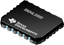
SN54LS595 具有输出锁存器的 8 位移位寄存器
 These devices each contain an 8-bit serial-in, parallel-out shift register that feeds an 8-bit D-type storage register. The storage register has parallel 3-state ('LS595) or open-collector ('LS596) outputs. Separate clocks are provided for both the shift register and the storage register. The shift register has a direct-overriding clear, serial input, and serial output pins for cascading.
Both the shift register and storage register clocks are positive-edge triggered. If the user wishes to connect both clocks together, the shift register state will always be one clock pulse ahead of the storage register
| SN54LS595 | |
| Technology Family | LS |
| Rating | Military |
SN54LS595 特性
- 8-Bit Serial-In, Parallel-Out Shift Registers with Storage
- Choice of 3-State ('LS595) or Open-Collector ('LS596) Parallel Outputs
- Shift Register Has Direct Clear
- Accurate Shift Frequency:DC to 20 MHz
SN54LS595 芯片订购指南
| 器件 | 状态 | 温度 | 价格 | 封装 | 引脚 | 封装数量 | 封装载体 | 丝印标记 |
| SN54LS595J | ACTIVE | -55 to 125 | 16.23 | 1ku | CDIP (J) | 16 | 1 | TUBE | |
| SNJ54LS595FK | ACTIVE | -55 to 125 | 17.37 | 1ku | LCCC (FK) | 20 | 1 | TUBE | |
| SNJ54LS595J | ACTIVE | -55 to 125 | 23.81 | 1ku | CDIP (J) | 16 | 1 | TUBE | |
| SNJ54LS595W | ACTIVE | -55 to 125 | 16.23 | 1ku | CFP (W) | 16 | 1 | TUBE |
SN54LS595 质量与无铅数据
| 器件 | 环保计划* | 铅/焊球涂层 | MSL 等级/回流焊峰 | 环保信息与无铅 (Pb-free) | DPPM / MTBF / FIT 率 |
| SN54LS595J | TBD | A42 | N/A for Pkg Type | SN54LS595J | SN54LS595J |
| SNJ54LS595FK | TBD | POST-PLATE | N/A for Pkg Type | SNJ54LS595FK | SNJ54LS595FK |
| SNJ54LS595J | TBD | A42 | N/A for Pkg Type | SNJ54LS595J | SNJ54LS595J |
| SNJ54LS595W | TBD | Call TI | N/A for Pkg Type | SNJ54LS595W | SNJ54LS595W |
SN54LS595 应用技术支持与电子电路设计开发资源下载
- SN54LS595 数据资料 dataSheet 下载.PDF
- TI 德州仪器触发器/锁存器/寄存器产品选型与价格 . xls
- Shelf-Life Evaluation of Lead-Free Component Finishes (PDF 1305 KB)
- Understanding and Interpreting Standard-Logic Data Sheets (PDF 857 KB)
- TI IBIS File Creation, Validation, and Distribution Processes (PDF 380 KB)
- Implications of Slow or Floating CMOS Inputs (PDF 101 KB)
- CMOS Power Consumption and CPD Calculation (PDF 89 KB)
- Designing With Logic (PDF 186 KB)
- Live Insertion (PDF 150 KB)
- Input and Output Characteristics of Digital Integrated Circuits (PDF 1708 KB)
- Using High Speed CMOS and Advanced CMOS in Systems With Multiple Vcc (PDF 43 KB)
- HiRel Unitrode Power Management Brochure (PDF 206 KB)
- LOGIC Pocket Data Book (PDF 6001 KB)
- HiRel Unitrode Power Management Brochure (PDF 206 KB)
- Logic Cross-Reference (PDF 2938 KB)
