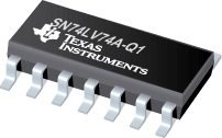
SN74LV74A-Q1 汽车类双路上升沿 D 类触发器
 This dual positive-edge-triggered D-type flip-flop is designed for 2-V to 5.5-V VCC operation.
A low level at the preset (PRE) or clear (CLR) inputs sets or resets the outputs, regardless of the levels of the other inputs. When PRE and CLR are inactive (high), data at the data (D) inputs meeting the setup-time requirements is transferred to the outputs on the positive-going edge of the clock pulse. Clock triggering occurs at a voltage level and is not directly related to the rise time of the clock pulse. Following the hold-time interval, data at the D input can be changed without affecting the levels at the outputs.
This device is fully specified for partial-power-down applications using Ioff. The Ioff circuitry disables the outputs, preventing damaging current backflow through the device when it is powered down
| SN74LV74A-Q1 | |
| Voltage Nodes(V) | 2.5, 3.5, 5 |
| Rating | Automotive |
SN74LV74A-Q1 特性
- Qualified for Automotive Applications
- 2-V to 5.5-V VCC Operation
- Max tpd of 13 ns at 5 V
- Typical VOLP (Output Ground Bounce) <0.8 V at VCC = 3.3 V, TA = 25°C
- Typical VOHV (Output VOH Undershoot) >2.3 V at VCC = 3.3 V, TA = 25°C
- Support Mixed-Mode Voltage Operation on All Ports
- Ioff Supports Partial-Power-Down Mode Operation
- Latch-Up Performance Exceeds 250 mA Per JESD 17
- ESD Protection Exceeds JESD 22
- 2000-V Human-Body Model (A114-A)
- 200-V Machine Model (A115-A)
- 1000-V Charged-Device Model (C101)
SN74LV74A-Q1 芯片订购指南
| 器件 | 状态 | 温度 | 价格(美元) | 封装 | 引脚 | 封装数量 | 封装载体 | 丝印标记 |
| SN74LV74AQDRG4Q1 | ACTIVE | -40 to 125 | 0.25 | 1ku | SOIC (D) | 14 | 2500 | |
| SN74LV74AQDRQ1 | ACTIVE | -40 to 125 | 0.25 | 1ku | SOIC (D) | 14 | 2500 | |
| SN74LV74AQPWRG4Q1 | ACTIVE | -40 to 125 | 0.25 | 1ku | TSSOP (PW) | 14 | 2000 | |
| SN74LV74AQPWRQ1 | ACTIVE | -40 to 125 | 0.25 | 1ku | TSSOP (PW) | 14 | 2000 |
SN74LV74A-Q1 质量与无铅数据
| 器件 | 环保计划* | 铅/焊球涂层 | MSL 等级/回流焊峰 | 环保信息与无铅 (Pb-free) | DPPM / MTBF / FIT 率 |
| SN74LV74AQDRG4Q1 | Green (RoHS & no Sb/Br) | CU NIPDAU | Level-1-260C-UNLIM | SN74LV74AQDRG4Q1 | SN74LV74AQDRG4Q1 |
| SN74LV74AQDRQ1 | Green (RoHS & no Sb/Br) | CU NIPDAU | Level-1-260C-UNLIM | SN74LV74AQDRQ1 | SN74LV74AQDRQ1 |
| SN74LV74AQPWRG4Q1 | Green (RoHS & no Sb/Br) | CU NIPDAU | Level-1-260C-UNLIM | SN74LV74AQPWRG4Q1 | SN74LV74AQPWRG4Q1 |
| SN74LV74AQPWRQ1 | Green (RoHS & no Sb/Br) | CU NIPDAU | Level-1-260C-UNLIM | SN74LV74AQPWRQ1 | SN74LV74AQPWRQ1 |
SN74LV74A-Q1 应用技术支持与电子电路设计开发资源下载
- SN74LV74A-Q1 数据资料 dataSheet 下载.PDF
- TI 德州仪器触发器/锁存器/寄存器产品选型与价格 . xls
- Shelf-Life Evaluation of Lead-Free Component Finishes (PDF 1305 KB)
- Understanding and Interpreting Standard-Logic Data Sheets (PDF 857 KB)
- TI IBIS File Creation, Validation, and Distribution Processes (PDF 380 KB)
- Implications of Slow or Floating CMOS Inputs (PDF 101 KB)
- CMOS Power Consumption and CPD Calculation (PDF 89 KB)
- Designing With Logic (PDF 186 KB)
- Live Insertion (PDF 150 KB)
- Input and Output Characteristics of Digital Integrated Circuits (PDF 1708 KB)
- Using High Speed CMOS and Advanced CMOS in Systems With Multiple Vcc (PDF 43 KB)
- HiRel Unitrode Power Management Brochure (PDF 206 KB)
- LOGIC Pocket Data Book (PDF 6001 KB)
- HiRel Unitrode Power Management Brochure (PDF 206 KB)
- Logic Cross-Reference (PDF 2938 KB)
