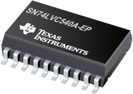
SN74LVC540A-EP 具有三态输出的增强型产品八路缓冲器/驱动器

The SN74LVC540A-EP octal buffer/driver is designed for 2.7-V to 3.6-V VCC operation.
This device is ideal for driving bus lines or buffer-memory address registers. This device features inputs and outputs on opposite sides of the package that facilitate printed circuit board layout.
The 3-state control gate is a 2-input AND gate with active-low inputs so that, if either output-enable (OE1 or OE2) input is high, all outputs are in the high-impedance state.
Inputs can be driven from either 3.3-V or 5-V devices. This feature allows the use of this device as a translator in a mixed 3.3-V/5-V system environment.
This device is fully specified for partial-power-down applications using Ioff. The Ioff circuitry disables the outputs, preventing damaging current backflow through the device when it is powered down.
| SN74LVC540A-EP | |
| Voltage Nodes (V) | 3.3, 2.7 |
| Vcc range (V) | 2.0 to 3.6 |
| Input Level | TTL/CMOS |
| Output Level | LVTTL |
| No. of Outputs | 8 |
| Output Drive (mA) | -24/24 |
| tpd max (ns) | 5.3 |
| Static Current | 0.01 |
| Logic | Inverting |
| Technology Family | LVC |
| Rating | HiRel Enhanced Product |
| Pin/Package | 20SOIC, 20TSSOP |
SN74LVC540A-EP 特性
- Controlled Baseline
- One Assembly/Test Site, One Fabrication Site
- Extended Temperature Performance of –40°C to 125°C
- Enhanced Diminishing Manufacturing Sources (DMS) Support
- Enhanced Product-Change Notification
- Qualification Pedigree
- Operates From 2 V to 3.6 V
- Inputs Accept Voltages to 5.5 V
- Max tpd of 5.3 ns at 3.3 V
- Typical VOLP (Output Ground Bounce) <0.8 V at VCC = 3.3 V, TA = 25°C
- Typical VOHV (Output VOH Undershoot) >2 V at VCC = 3.3 V, TA = 25°C
- Supports Mixed-Mode Signal Operation on All Ports (5-V Input/Output Voltage With 3.3-V VCC)
- Ioff Supports Partial-Power-Down Mode Operation
SN74LVC540A-EP 芯片订购指南
| 器件 | 状态 | 温度 | 价格(美元) | 封装 | 引脚 | 封装数量 | 封装载体 | 丝印标记 |
| SN74LVC540AQDWREP | ACTIVE | -40 to 125 | 0.42 | 1ku | SOIC (DW) | 20 | 2000 | LARGE T&R | |
| SN74LVC540AQPWREP | ACTIVE | -40 to 125 | 0.48 | 1ku | TSSOP (PW) | 20 | 2000 | LARGE T&R | |
| V62/04665-01XE | ACTIVE | -40 to 125 | 0.42 | 1ku | SOIC (DW) | 20 | 2000 | LARGE T&R | |
| V62/04665-01YE | ACTIVE | -40 to 125 | 0.48 | 1ku | TSSOP (PW) | 20 | 2000 | LARGE T&R |
SN74LVC540A-EP 应用手册
SN74LVC540A-EP 质量与无铅数据
| 器件 | 环保计划* | 铅/焊球涂层 | MSL 等级/回流焊峰 | 环保信息与无铅 (Pb-free) | DPPM / MTBF / FIT 率 |
| SN74LVC540AQDWREP | Green (RoHS & no Sb/Br) | CU NIPDAU | Level-1-260C-UNLIM | SN74LVC540AQDWREP | SN74LVC540AQDWREP |
| SN74LVC540AQPWREP | Green (RoHS & no Sb/Br) | CU NIPDAU | Level-1-260C-UNLIM | SN74LVC540AQPWREP | SN74LVC540AQPWREP |
| V62/04665-01XE | Green (RoHS & no Sb/Br) | CU NIPDAU | Level-1-260C-UNLIM | V62/04665-01XE | V62/04665-01XE |
| V62/04665-01YE | Green (RoHS & no Sb/Br) | CU NIPDAU | Level-1-260C-UNLIM | V62/04665-01YE | V62/04665-01YE |
SN74LVC540A-EP 应用技术支持与电子电路设计开发资源下载
- SN74LVC540A-EP 数据资料 dataSheet 下载.PDF
- TI 德州仪器缓冲器、驱动器/收发器产品选型与价格 . xls
- (选择指南)逻辑器件指南 2009 (Rev. Z)
- (选择指南)小尺寸逻辑器件指南 (Rev. D)
- (用户指南)LOGIC Pocket Data Book
- (用户指南)Signal Switch Data Book
- (用户指南)LVC and LV Low-Voltage CMOS Logic Data Book
- (解决方案指南)2008年第一季度通信基础设施方案指南 (Rev. G)
- (解决方案指南)Communications Infrastructure Solutions Guide 1Q2010
