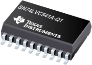
SN74LVC541A-Q1 汽车类具有三态输出的八路缓冲器/驱动器
 SN74LVC541A-Q1 描述
The SN74LVC541A octal buffer/driver is designed for 2.7-V to 3.6-V VCC operation.
The device is ideal for driving bus lines or buffering memory address registers.
This device features inputs and outputs on opposite sides of the package to facilitate printed circuit board layout.
The 3-state control gate is a 2-input AND gate with active-low inputs so that, if either output enable (OE1 or OE2) input is high, all eight outputs are in the high-impedance state.
Inputs can be driven from either 3.3-V or 5-V devices. This feature allows the use of this device as a translator in a mixed 3.3-V/5-V system environment.
This device is fully specified for partial-power-down applications using Ioff. The Ioff circuitry disables the outputs, preventing damaging current backflow through the device when it is powered down.
To ensure the high-impedance state during power up or power down, OE should be tied to VCC through a pullup resistor; the minimum value of the resistor is determined by the current-sinking capability of the driver
| SN74LVC541A-Q1 | |
| Voltage Nodes(V) | 3.3, 2.7 |
| Vcc range(V) | 2.0 to 3.6 |
| Logic | True |
| Input Level | TTL/CMOS |
| Output Level | LVTTL |
| Output Drive(mA) | -24/24 |
| No. of Outputs | 8 |
| tpd max(ns) | 5.1 |
| Static Current | 0.01 |
| Rating | Automotive |
| Technology Family | LVC |
SN74LVC541A-Q1 特性
- Qualified for Automotive Applications
- ESD Protection Exceeds 2000 V Per MIL-STD-883, Method 3015; Exceeds 200 V Using Machine Model (C = 200 pF, R = 0)
- Operates From 2 V to 3.6 V
- Inputs Accept Voltages to 5.5 V
- Max tpd of 5.1 ns at 3.3 V
- Typical VOLP (Output Ground Bounce) < 0.8 V at VCC = 3.3 V, TA = 25°C
- Typical VOHV (Output VOH Undershoot)> 2 V at VCC = 3.3 V, TA = 25°C
- Supports Mixed-Mode Signal Operation on All Ports (5-V Input/Output Voltage With 3.3-V VCC)
SN74LVC541A-Q1 应用技术支持与电子电路设计开发资源下载
- SN74LVC541A-Q1 数据资料 dataSheet 下载.PDF
- TI 德州仪器缓冲器、驱动器/收发器产品选型与价格 . xls
- CMOS 非缓冲反向器在振荡器电路中的使用 (PDF 951 KB)
- Semiconductor Packing Methodology (PDF 3005 KB)
- 逻辑产品选择指南 2006/2007 (修订版 Z)(4462KB)
- 标准线性和逻辑产品 5 分钟指南 (786KB)
- 了解和解释标准逻辑数据表
- LOGIC Pocket Data Book (PDF 6001 KB)
- HiRel Unitrode Power Management Brochure (PDF 206 KB)
- Logic Cross-Reference (PDF 2938 KB)
