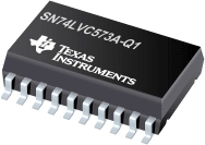
SN74LVC573A-Q1 汽车类具有三态输出的八路透明 D 类锁存器
 The SN74LVC573A octal transparent D-type latch is designed for 2.7-V to 3.6-V VCC operation.
This device features 3-state outputs designed specifically for driving highly capacitive or relatively low-impedance loads. It is particularly suitable for implementing buffer registers, input/output (I/O) ports, bidirectional bus drivers, and working registers.
While the latch-enable (LE) input is high, the Q outputs follow the data (D) inputs. When LE is taken low, the Q outputs are latched at the logic levels at the D inputs.
A buffered output-enable (OE) input can be used to place the eight outputs in either a normal logic state (high or low logic levels) or the high-impedance state. In the high-impedance state, the outputs neither load nor drive the bus lines significantly. The high-impedance state and increased drive provide the capability to drive bus lines without interface or pullup components.
OE does not affect the internal operations of the latches. Old data can be retained or new data can be entered while the outputs are in the high-impedance state.
This device is fully specified for partial-power-down applications using Ioff. The Ioff circuitry disables the outputs, preventing damaging current backflow through the device when it is powered down.
To ensure the high-impedance state during power up or power down, OE should be tied to VCC through a pullup resistor; the minimum value of the resistor is determined by the current-sinking capability of the driver.
Inputs can be driven from either 3.3-V or 5-V devices. This feature allows the use of this device as a translator in a mixed 3.3-V/5-V system environment
| SN74LVC573A-Q1 | |
| Voltage Nodes(V) | 3.3, 2.7 |
| Vcc range(V) | 2.0 to 3.6 |
| Input Level | TTL/CMOS |
| Output Level | LVTTL |
| Logic | True |
| No. of Outputs | 8 |
| Output Drive(mA) | -24/24 |
| Static Current | 0.01 |
| th(ns) | 2.5 |
| Technology Family | LVC |
| tsu(ns) | 2 |
| tpd max(ns) | 7.7 |
| Rating | Automotive |
SN74LVC573A-Q1 特性
- Qualified for Automotive Applications
- ESD Protection Exceeds 2000 V Per MIL-STD-883, Method 3015; Exceeds 200 V Using Machine Model (C = 200 pF, R = 0)
- Operates From 2 V to 3.6 V
- Inputs Accept Voltages to 5.5 V
- Max tpd of 6.9 ns at 3.3 V
- Typical VOLP (Output Ground Bounce) < 0.8 V at VCC = 3.3 V, TA = 25°C
- Typical VOHV (Output VOH Undershoot)> 2 V at VCC = 3.3 V, TA = 25°C
- Supports Mixed-Mode Signal Operation on All Ports (5-V Input/Output Voltage With 3.3-V VCC)
- Ioff Supports Partial-Power-Down Mode Operation
SN74LVC573A-Q1 芯片订购指南
| 器件 | 状态 | 温度 | 价格(美元) | 封装 | 引脚 | 封装数量 | 封装载体 | 丝印标记 |
| CLVC573AQDWRG4Q1 | ACTIVE | -40 to 125 | 0.28 | 1ku | SOIC (DW) | 20 | 2000 | |
| CLVC573AQPWRG4Q1 | ACTIVE | -40 to 125 | 0.28 | 1ku | TSSOP (PW) | 20 | 2000 | |
| SN74LVC573AQDWRQ1 | ACTIVE | -40 to 125 | 0.28 | 1ku | SOIC (DW) | 20 | 2000 | |
| SN74LVC573AQPWRQ1 | ACTIVE | -40 to 125 | 0.28 | 1ku | TSSOP (PW) | 20 | 2000 |
SN74LVC573A-Q1 质量与无铅数据
| 器件 | 环保计划* | 铅/焊球涂层 | MSL 等级/回流焊峰 | 环保信息与无铅 (Pb-free) | DPPM / MTBF / FIT 率 |
| CLVC573AQDWRG4Q1 | Green (RoHS & no Sb/Br) | CU NIPDAU | Level-1-260C-UNLIM | CLVC573AQDWRG4Q1 | CLVC573AQDWRG4Q1 |
| CLVC573AQPWRG4Q1 | Green (RoHS & no Sb/Br) | CU NIPDAU | Level-1-260C-UNLIM | CLVC573AQPWRG4Q1 | CLVC573AQPWRG4Q1 |
| SN74LVC573AQDWRQ1 | Green (RoHS & no Sb/Br) | CU NIPDAU | Level-1-260C-UNLIM | SN74LVC573AQDWRQ1 | SN74LVC573AQDWRQ1 |
| SN74LVC573AQPWRQ1 | Green (RoHS & no Sb/Br) | CU NIPDAU | Level-1-260C-UNLIM | SN74LVC573AQPWRQ1 | SN74LVC573AQPWRQ1 |
SN74LVC573A-Q1 应用技术支持与电子电路设计开发资源下载
- SN74LVC573A-Q1 数据资料 dataSheet 下载.PDF
- TI 德州仪器触发器/锁存器/寄存器产品选型与价格 . xls
- Shelf-Life Evaluation of Lead-Free Component Finishes (PDF 1305 KB)
- Understanding and Interpreting Standard-Logic Data Sheets (PDF 857 KB)
- TI IBIS File Creation, Validation, and Distribution Processes (PDF 380 KB)
- Implications of Slow or Floating CMOS Inputs (PDF 101 KB)
- CMOS Power Consumption and CPD Calculation (PDF 89 KB)
- Designing With Logic (PDF 186 KB)
- Live Insertion (PDF 150 KB)
- Input and Output Characteristics of Digital Integrated Circuits (PDF 1708 KB)
- Using High Speed CMOS and Advanced CMOS in Systems With Multiple Vcc (PDF 43 KB)
- HiRel Unitrode Power Management Brochure (PDF 206 KB)
- LOGIC Pocket Data Book (PDF 6001 KB)
- HiRel Unitrode Power Management Brochure (PDF 206 KB)
- Logic Cross-Reference (PDF 2938 KB)
