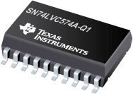
SN74LVC574A-Q1 汽车类具有三态输出的八路边沿 D 类触发器
 The SN74LVC574A octal edge-triggered D-type flip-flop is designed for 2.7-V to 3.6-V VCC operation.
This device features 3-state outputs designed specifically for driving highly capacitive or relatively low-impedance loads. It is particularly suitable for implementing buffer registers, I/O ports, bidirectional bus drivers, and working registers.
On the positive transition of the clock (CLK) input, the Q outputs are set to the logic levels at the data (D) inputs.
A buffered output-enable (OE) input can be used to place the eight outputs in either a normal logic state (high or low logic levels) or the high-impedance state. In the high-impedance state, the outputs neither load nor drive the bus lines significantly. The high-impedance state and increased drive provide the capability to drive bus lines without interface or pullup components.
OE does not affect the internal operations of the flip-flops. Old data can be retained or new data can be entered while the outputs are in the high-impedance state.
This device is fully specified for partial-power-down applications using Ioff. The Ioff circuitry disables the outputs, preventing damaging current backflow through the device when it is powered down.
To ensure the high-impedance state during power up or power down, OE should be tied to VCC through a pullup resistor; the minimum value of the resistor is determined by the current-sinking capability of the driver.
Inputs can be driven from either 3.3-V or 5-V devices. This feature allows the use of thIs device as a translator in a mixed 3.3-V/5-V system environment
| SN74LVC574A-Q1 | |
| Voltage Nodes(V) | 3.3, 2.7 |
| Vcc range(V) | 2.0 to 3.6 |
| Input Level | TTL/CMOS |
| Output Level | LVTTL |
| Output Drive(mA) | -24/24 |
| No. of Outputs | 8 |
| Static Current | 0.01 |
| th(ns) | 2 |
| tpd max(ns) | 8 |
| tsu(ns) | 2 |
| Logic | True |
| Technology Family | LVC |
| Rating | Automotive |
SN74LVC574A-Q1 特性
- Qualified for Automotive Applications
- ESD Protection Exceeds 2000 V Per
MIL-STD-883, Method 3015; Exceeds 200 V Using Machine Model (C = 200 pF, R = 0) - Operates From 2 V to 3.6 V
- Inputs Accept Voltages to 5.5 V
- Max tpd of 7 ns at 3.3 V
- Typical VOLP (Output Ground Bounce) < 0.8 V at VCC = 3.3 V, TA = 25°C
- Typical VOHV (Output VOH Undershoot) > 2 V at VCC = 3.3 V, TA = 25°C
- Supports Mixed-Mode Signal Operation on All Ports (5-V Input/Output Voltage With 3.3-V VCC)
- Ioff Supports Partial-Power-Down Mode Operation
SN74LVC574A-Q1 芯片订购指南
| 器件 | 状态 | 温度 | 价格(美元) | 封装 | 引脚 | 封装数量 | 封装载体 | 丝印标记 |
| CLVC574AQDWRG4Q1 | ACTIVE | -40 to 125 | 0.28 | 1ku | SOIC (DW) | 20 | 2000 | |
| CLVC574AQPWRG4Q1 | ACTIVE | -40 to 125 | 0.28 | 1ku | TSSOP (PW) | 20 | 2000 | |
| SN74LVC574AQDWRQ1 | ACTIVE | -40 to 125 | 0.28 | 1ku | SOIC (DW) | 20 | 2000 | |
| SN74LVC574AQPWRQ1 | ACTIVE | -40 to 125 | 0.28 | 1ku | TSSOP (PW) | 20 | 2000 |
SN74LVC574A-Q1 质量与无铅数据
| 器件 | 环保计划* | 铅/焊球涂层 | MSL 等级/回流焊峰 | 环保信息与无铅 (Pb-free) | DPPM / MTBF / FIT 率 |
| CLVC574AQDWRG4Q1 | Green (RoHS & no Sb/Br) | CU NIPDAU | Level-1-260C-UNLIM | CLVC574AQDWRG4Q1 | CLVC574AQDWRG4Q1 |
| CLVC574AQPWRG4Q1 | Green (RoHS & no Sb/Br) | CU NIPDAU | Level-1-260C-UNLIM | CLVC574AQPWRG4Q1 | CLVC574AQPWRG4Q1 |
| SN74LVC574AQDWRQ1 | Green (RoHS & no Sb/Br) | CU NIPDAU | Level-1-260C-UNLIM | SN74LVC574AQDWRQ1 | SN74LVC574AQDWRQ1 |
| SN74LVC574AQPWRQ1 | Green (RoHS & no Sb/Br) | CU NIPDAU | Level-1-260C-UNLIM | SN74LVC574AQPWRQ1 | SN74LVC574AQPWRQ1 |
SN74LVC574A-Q1 应用技术支持与电子电路设计开发资源下载
- SN74LVC574A-Q1 数据资料 dataSheet 下载.PDF
- TI 德州仪器触发器/锁存器/寄存器产品选型与价格 . xls
- Shelf-Life Evaluation of Lead-Free Component Finishes (PDF 1305 KB)
- Understanding and Interpreting Standard-Logic Data Sheets (PDF 857 KB)
- TI IBIS File Creation, Validation, and Distribution Processes (PDF 380 KB)
- Implications of Slow or Floating CMOS Inputs (PDF 101 KB)
- CMOS Power Consumption and CPD Calculation (PDF 89 KB)
- Designing With Logic (PDF 186 KB)
- Live Insertion (PDF 150 KB)
- Input and Output Characteristics of Digital Integrated Circuits (PDF 1708 KB)
- Using High Speed CMOS and Advanced CMOS in Systems With Multiple Vcc (PDF 43 KB)
- HiRel Unitrode Power Management Brochure (PDF 206 KB)
- LOGIC Pocket Data Book (PDF 6001 KB)
- HiRel Unitrode Power Management Brochure (PDF 206 KB)
- Logic Cross-Reference (PDF 2938 KB)
