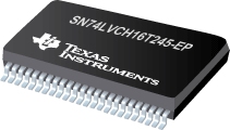
SN74LVCH16T245-EP 增强型产品 16 位双电源总线收发器,具有可配置电压转换和三态输出
 This 16-bit noninverting bus transceiver uses two separate configurable power-supply rails. The A port is designed to track VCCA. VCCA accepts any supply voltage from 1.65 V to 5.5 V. The B port is designed to track VCCB. VCCB accepts any supply voltage from 1.65 V to 5.5 V. This allows for universal low-voltage bidirectional translation between any of the 1.8-V, 2.5-V, 3.3-V, and 5-V voltage nodes.
The SN74LVCH16T245 is designed so that the control pins (1DIR, 2DIR, 1OE, and 2OE) are supplied by VCCA.
The SN74LVCH16T245 is designed for asynchronous communication between two data buses. The logic levels of the direction-control (DIR) input and the output-enable (OE) input activate either the B-port outputs or the A-port outputs or place both output ports into the high-impedance mode. The device transmits data from the A bus to the B bus when the B-port outputs are activated, and from the B bus to the A bus when the A-port outputs are activated. The input circuitry on both A and B ports is always active and must have a logic HIGH or LOW level applied to prevent excess ICC and ICCZ.
Active bus-hold circuitry holds unused or undriven data inputs at a valid logic state. Use of pullup or pulldown resistors with the bus-hold circuitry is not recommended.
This device is fully specified for partial-power-down applications using Ioff. The Ioff circuitry disables the outputs, preventing damaging current backflow through the device when it is powered down.
The VCC isolation feature ensures that if either VCC input is at GND, then all outputs are in the high-impedance state. The bus-hold circuitry on the powered-up side always stays active.
To ensure the high-impedance state during power up or power down, OE should be tied to VCC through a pullup resistor; the minimum value of the resistor is determined by the current-sinking capability of the driver
| SN74LVCH16T245-EP | |
| Voltage Nodes(V) | 1.8,2.5,3.3,5 |
| Vcc range(V) | 1.65 to 5.5 |
| Input Level | TTL/CMOS |
| Output Level | LVTTL |
| Logic | True |
| No. of Outputs | 16 |
| Output Drive(mA) | -32,32 |
| Technology Family | LVC |
| Pin/Package | 48TSSOP, 48TVSOP |
| Operating Temperature Range(°C) | -55 to 125 |
| Rating | HiRel Enhanced Product |
SN74LVCH16T245-EP 特性
- Control Inputs VIH/VIL Levels Are Referenced to VCCA Voltage
- VCC Isolation Feature – If Either VCC Input Is at GND,
All Outputs Are in the High-Impedance State - Overvoltage-Tolerant Inputs/Outputs Allow
Mixed-Voltage-Mode Data Communications - Fully Configurable Dual-Rail Design Allows Each Port to Operate
Over the Full 1.65-V to 5.5-V Power-Supply Range - Bus Hold on Data Inputs Eliminates the Need for
External Pullup/Pulldown Resistors - Ioff Supports Partial-Power-Down Mode Operation
- Latch-Up Performance Exceeds 100 mA Per JESD 78, Class II
- ESD Protection Exceeds JESD 22
- 2000-V Human-Body Model (A114-A)
- 200-V Machine Model (A115-A)
- 1000-V Charged-Device Model (C101)
- SUPPORTS DEFENSE, AEROSPACE, AND MEDICAL APPLICATIONS
- Controlled Baseline
- One Assembly/Test Site
- One Fabrication Site
- Available in Military (–55°C/125°C) Temperature Ranges(1)
- Extended Product Life Cycle
- Extended Product-Change Notification
- Product Traceability
SN74LVCH16T245-EP 芯片订购指南
| 器件 | 状态 | 温度 | 价格(美元) | 封装 | 引脚 | 封装数量 | 封装载体 | 丝印标记 |
| CLVCH16T245MDGGREP | ACTIVE | -55 to 125 | 3.50 | 100u | TSSOP (DGG) | 48 | 2000 | LARGE T&R | |
| V62/09605-01XE | ACTIVE | -55 to 125 | 3.50 | 100u | TSSOP (DGG) | 48 | 2000 | LARGE T&R |
SN74LVCH16T245-EP 质量与无铅数据
| 器件 | 环保计划* | 铅/焊球涂层 | MSL 等级/回流焊峰 | 环保信息与无铅 (Pb-free) | DPPM / MTBF / FIT 率 |
| CLVCH16T245MDGGREP | Green (RoHS & no Sb/Br) | CU NIPDAU | Level-1-260C-UNLIM | CLVCH16T245MDGGREP | CLVCH16T245MDGGREP |
| V62/09605-01XE | Green (RoHS & no Sb/Br) | CU NIPDAU | Level-1-260C-UNLIM | V62/09605-01XE | V62/09605-01XE |
SN74LVCH16T245-EP 应用技术支持与电子电路设计开发资源下载
- SN74LVCH16T245-EP 数据资料 dataSheet 下载.PDF
- TI 德州仪器电压电平转换产品选型与价格 . xls
- Shelf-Life Evaluation of Lead-Free Component Finishes (PDF 1305 KB)
- Understanding and Interpreting Standard-Logic Data Sheets (PDF 857 KB)
- TI IBIS File Creation, Validation, and Distribution Processes (PDF 380 KB)
- Implications of Slow or Floating CMOS Inputs (PDF 101 KB)
- CMOS Power Consumption and CPD Calculation (PDF 89 KB)
- Designing With Logic (PDF 186 KB)
- Live Insertion (PDF 150 KB)
- Input and Output Characteristics of Digital Integrated Circuits (PDF 1708 KB)
- Using High Speed CMOS and Advanced CMOS in Systems With Multiple Vcc (PDF 43 KB)
- HiRel Unitrode Power Management Brochure (PDF 206 KB)
- LOGIC Pocket Data Book (PDF 6001 KB)
- HiRel Unitrode Power Management Brochure (PDF 206 KB)
- Logic Cross-Reference (PDF 2938 KB)
