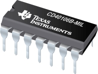
CD40106B-MIL CMOS 六路施密特触发器

CD40106B consists of six Schmitt-trigger circuits. Each circuit functions as an inverter with Schmitt-trigger action on the input. The trigger switches at different points for positive- and negative-going signals. The difference between the positive-going voltage (VP) and the negative-going voltage (VN) is defined as hysteresis voltage (VH) (see Fig. 6).
The CD40106B types are supplied in 14-lead hermetic dual-in-line ceramic packages (F3A suffix), 14-lead dual-in-line plastic packages (E suffix), 14-lead small-outline packages (M, MT, M96, and NSR suffixes), and 14-lead thin shrink small-outline packages (PW and PWR suffixes).
|
CD40106B-MIL |
| Voltage Nodes (V) |
5, 10, 15 |
| Vcc range (V) |
3.0 to 18.0 |
| Input Level |
CMOS |
| Output Level |
CMOS |
| No. of Outputs |
6 |
| Output Drive (mA) |
-1/1 |
| tpd max (ns) |
280 |
| Static Current |
0.001 |
| Logic |
Inverting |
| Technology Family |
CD4000 |
| Rating |
Military |
| Pin/Package |
14CDIP |
CD40106B-MIL 特性
- Schmitt-trigger action with no external components
- Hysteresis voltage (typ.) at 0.9 V at VDD = 5 V, 2.3 V at VDD = 10 V, and 3.5 V at VDD = 15 V
- Noise immunity greater than 50%
- No limit on input rise and fall times
- Standardized, symmetrical output characteristics
- 100% tested for quiescent current at 20 V
- Maximum input current of 1 µA at 18 V over full package-temperature range; 100 nA at 18 V and 25°C
- Low VDD to VSS current during slow input ramp
- 5-V, 10-V, and 15-V parametric ratings
- Meets all requirements of JEDEC Tentative Standard No. 13B, "Standard Specifications for Description of 'B' Series CMOS Devices"
- Applications:
- Wave and pulse shapers
- High-noise-environment systems
- Monostable multivibrators
- Astable multivibrators
CD40106B-MIL 芯片订购指南
| 器件 |
状态 |
温度 |
价格(美元) |
封装 | 引脚 |
封装数量 | 封装载体 |
丝印标记 |
| CD40106BF |
ACTIVE |
-55 to 125 |
3.44 | 1ku |
CDIP (J) | 14 |
1 | TUBE |
|
| CD40106BF3A |
ACTIVE |
-55 to 125 |
3.72 | 1ku |
CDIP (J) | 14 |
1 | TUBE |
|
CD40106B-MIL 质量与无铅数据
| 器件 |
环保计划* |
铅/焊球涂层 |
MSL 等级/回流焊峰 |
环保信息与无铅 (Pb-free) |
DPPM / MTBF / FIT 率 |
| CD40106BF |
TBD |
A42 |
N/A for Pkg Type |
CD40106BF |
CD40106BF |
| CD40106BF3A |
TBD |
A42 |
N/A for Pkg Type |
CD40106BF3A |
CD40106BF3A |
CD40106B-MIL 应用技术支持与电子电路设计开发资源下载
- CD40106B-MIL 数据资料 dataSheet 下载.PDF
- TI 德州仪器缓冲器、驱动器/收发器产品选型与价格 . xls
- (选择指南)逻辑器件指南 2009 (Rev. Z)
- (用户指南)LOGIC Pocket Data Book
- (用户指南)Signal Switch Data Book
- Logic Cross-Reference (PDF 2938 KB)

