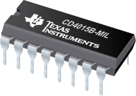
CD4015B-MIL CMOS 双路 4 级静态移位寄存器
 CD4015B consists of two identical, independent, 4-stage serial-input/parallel-output registers. Each register has independent CLOCK and RESET inputs as well as a single serial DATA input. "Q" outputs are available from each of the four stages on both registers. All register stages are D-type, master-slave flip-flops. The logic level present at the DATA input is transferred into the first register stage and shifted over one stage at each positive-going clock transition. Resetting of all stages is accomplished by a high level on the reset line. Register expansion to 8 stages using one CD4015B-MIL package, or to more than 8 stages using additional CD4015B-MIL’s is possible.
The CD4015B-MIL-series types are supplied in 16-lead hermetic dual-in-line ceramic packages (F3A suffix), 16-lead dual-in-line plastic package (E suffix), 16-lead small-outline packages (M, M96, MT, and NSR suffixes), and 16-lead thin shrink small-outline packages (PW and PWR suffixes).
|
CD4015B-MIL |
| Voltage Nodes(V) |
5, 10, 15 |
| Technology Family |
CD4000 |
| Rating |
Catalog |
CD4015B-MIL 特性
- Medium speed operation...12 MHz (typ.) clock rate at VDD – VSS = 10 V
- Fully static operation
- 8 master-slave flip-flops plus input and output buffering
- 100% tested for quiescent current at 20 V
- 5-V, 10-V, and 15-V parametric ratings
- Standardized, symmetrical output characteristics
- Maximum input current of 1 µA at 18 V over full package-temperature range; 100 nA at 18 V and 25°C
- Noise margin (full package-temperature range) =
- 1 V at VDD = 5 V
- 2 V at VDD = 10 V
- 2.5 V at VDD = 15 V
- Meets all requirements of JEDEC Tentative Standard No. 13B, "Standard Specifications for Description of ’B’ Series CMOS Devices"
- Applications:
- Serial-input/parallel-output data queueing
- Serial to parallel data conversion
- General-purpose register
CD4015B-MIL 芯片订购指南
| 器件 |
状态 |
温度 |
价格 |
封装 | 引脚 |
封装数量 | 封装载体 |
丝印标记 |
| CD4015BF |
ACTIVE |
-55 to 125 |
4.33 | 1ku |
CDIP (JT) | 16 |
1 | TUBE |
|
| CD4015BF3A |
ACTIVE |
-55 to 125 |
5.10 | 1ku |
CDIP (JT) | 16 |
1 | TUBE |
|
CD4015B-MIL 质量与无铅数据
| 器件 |
环保计划* |
铅/焊球涂层 |
MSL 等级/回流焊峰 |
环保信息与无铅 (Pb-free) |
DPPM / MTBF / FIT 率 |
| CD4015BF |
TBD |
A42 |
N/A for Pkg Type |
CD4015BF |
CD4015BF |
| CD4015BF3A |
TBD |
A42 |
N/A for Pkg Type |
CD4015BF3A |
CD4015BF3A |
CD4015B-MIL 应用技术支持与电子电路设计开发资源下载
- CD4015B-MIL 数据资料 dataSheet 下载.PDF
- TI 德州仪器触发器/锁存器/寄存器产品选型与价格 . xls
- Shelf-Life Evaluation of Lead-Free Component Finishes (PDF 1305 KB)
- Understanding and Interpreting Standard-Logic Data Sheets (PDF 857 KB)
- TI IBIS File Creation, Validation, and Distribution Processes (PDF 380 KB)
- Implications of Slow or Floating CMOS Inputs (PDF 101 KB)
- CMOS Power Consumption and CPD Calculation (PDF 89 KB)
- Designing With Logic (PDF 186 KB)
- Live Insertion (PDF 150 KB)
- Input and Output Characteristics of Digital Integrated Circuits (PDF 1708 KB)
- Using High Speed CMOS and Advanced CMOS in Systems With Multiple Vcc (PDF 43 KB)
- HiRel Unitrode Power Management Brochure (PDF 206 KB)
- LOGIC Pocket Data Book (PDF 6001 KB)
- HiRel Unitrode Power Management Brochure (PDF 206 KB)
- Logic Cross-Reference (PDF 2938 KB)
 CD4015B consists of two identical, independent, 4-stage serial-input/parallel-output registers. Each register has independent CLOCK and RESET inputs as well as a single serial DATA input. "Q" outputs are available from each of the four stages on both registers. All register stages are D-type, master-slave flip-flops. The logic level present at the DATA input is transferred into the first register stage and shifted over one stage at each positive-going clock transition. Resetting of all stages is accomplished by a high level on the reset line. Register expansion to 8 stages using one CD4015B-MIL package, or to more than 8 stages using additional CD4015B-MIL’s is possible.