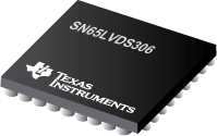
SN65LVDS306 可编程 27 位显示屏串行接口发送器
 The SN65LVDS306 receiver deserializes FlatLink™3G-compliant serial input data to 27 parallel data outputs. The SN65LVDS306 receiver contains one shift register to load 30 bits from one serial input and latches the 24 pixel bits and 3 control bits out to the parallel CMOS outputs after checking the parity bit. If the parity check confirms correct parity, the channel parity error (CPE) output remains low. If a parity error is detected, the CPE output generates a high pulse while the data output bus disregards the newly-received pixel. Instead, the last data word is held on the output bus for another clock cycle.
The serial data and clock are received via sub-low-voltage differential signalling (SubLVDS) lines. The SN65LVDS306 supports three operating power modes (shutdown, standby, and active) to conserve power
|
SN65LVDS301 |
SN65LVDS302 |
SN65LVDS303 |
SN65LVDS304 |
SN65LVDS305 |
SN65LVDS306 |
SN65LVDS311 |
| Number of Parallel Outputs |
|
27 |
|
27 |
|
27 |
|
| Number of Parallel Inputs |
27 |
|
27 |
|
27 |
|
27 |
| Data Throughput(MB/s) |
1755 |
1755 |
810 |
810 |
405 |
405 |
1755 |
| Serial Data Receiver Channels |
|
3 |
|
2 |
|
1 |
|
| Serial Data Transmitter Channels |
3 |
|
2 |
|
1 |
|
3 |
| Type of Line Circuit |
subLVDS |
subLVDS |
subLVDS |
subLVDS |
subLVDS |
subLVDS |
subLVDS |
| Supply Voltage(s)(V) |
1.8 |
1.8 |
1.8 |
1.8 |
1.8 |
1.8 |
1.8 |
| PLL Frequency(MHz) |
4 - 65 |
4 - 65 |
4 - 30 |
4 - 30 |
4 - 15 |
4 - 15 |
4 - 65 |
| Footprint |
SN65LVDS301 |
SN65LVDS302 |
SN65LVDS301 |
SN65LVDS302 |
SN65LVDS301 |
SN65LVDS302 |
SN65LVDS311 |
| Operating Temperature Range(°C) |
-40 to 85 |
-40 to 85 |
-40 to 85 |
-40 to 85 |
-40 to 85 |
-40 to 85 |
-40 to 85 |
| Pin/Package |
80BGA MICROSTAR JUNIOR |
80BGA MICROSTAR JUNIOR |
80BGA MICROSTAR JUNIOR |
80BGA MICROSTAR JUNIOR |
80BGA MICROSTAR JUNIOR |
80BGA MICROSTAR JUNIOR |
49DSBGA |
SN65LVDS306 特性
- Serial Interface Technology
- Compatible With FlatLink™3G Such as SN65LVDS305
- Supports Video Interfaces up to 24-Bit RGB Data and 3 Control Bits Received Over One SubLVDS Differential Line
- SubLVDS Differential Voltage Levels
- Up to 405-Mbps Data Throughput
- Three Operating Modes to Conserve Power
- Active mode QVGA: 17 mW
- Typical Shutdown: 0.7 µW
- TypicalStandby Mode: 27 µW Typical
- Bus-Swap Function for PCB-Layout Flexibility
- ESD Rating > 4 kV (HBM)
- Pixel Clock Range of 4 MHz-15 MHz
- Failsafe on all CMOS Inputs
- Packaged in 5-mm × 5-mm MicroStar Junior µBGA® With 0,5-mm Ball Pitch
- Very Low EMI Meets SAE J1752/3 Kh-Spec
- APPLICATIONS
- Small Low-Emission Interface Between Graphics Controller and LCD Display
- Mobile Phones and Smart Phones
- Portable Multimedia Players
SN65LVDS306 芯片订购指南
SN65LVDS306 质量与无铅数据
| 器件 |
环保计划* |
铅/焊球涂层 |
MSL 等级/回流焊峰 |
环保信息与无铅 (Pb-free) |
DPPM / MTBF / FIT 率 |
| SN65LVDS306ZQE |
Green (RoHS & no Sb/Br) |
SNAGCU |
Level-3-260C-168 HR |
SN65LVDS306ZQE |
SN65LVDS306ZQE |
| SN65LVDS306ZQER |
Green (RoHS & no Sb/Br) |
SNAGCU |
Level-3-260C-168 HR |
SN65LVDS306ZQER |
SN65LVDS306ZQER |
SN65LVDS306 应用技术支持与电子电路设计开发资源下载
- SN65LVDS306 数据资料 dataSheet 下载.PDF
- TI 德州仪器FlatLink选型与价格 . xls
- 所选封装材料的热学和电学性质 (PDF 645 KB)
- Q1 2009 Issue Analog Applications Journal (slyt319.PDF, 1.39 MB)
- 使用 TI 的 SN65LVDS306 收发器改善 CAN 网络安全性 (zhct033.PDF, 299 KB)
- Isolated CAN Reference Design (PDF 48 KB)
- Isolated RS-485 Reference Design (PDF 80 KB)
- 无铅组件涂层的保存期评估 (PDF 1305 KB)
- Isolated CAN EVM User's Guide (PDF 1168 KB)
- Energy Harvesting: Solar Solutions Guide (PDF 409 KB)
- Analog Signal Chain Guide (8.62 MB)
- Industrial Interface IC Solutions (101 KB)
 The SN65LVDS306 receiver deserializes FlatLink™3G-compliant serial input data to 27 parallel data outputs. The SN65LVDS306 receiver contains one shift register to load 30 bits from one serial input and latches the 24 pixel bits and 3 control bits out to the parallel CMOS outputs after checking the parity bit. If the parity check confirms correct parity, the channel parity error (CPE) output remains low. If a parity error is detected, the CPE output generates a high pulse while the data output bus disregards the newly-received pixel. Instead, the last data word is held on the output bus for another clock cycle.