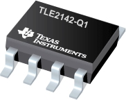
TLE2142-Q1 汽车类双路低噪声高速精密运算放大器
 The TLE2142 device is a high-performance, internally compensated operational amplifier built using the Texas Instruments complementary bipolar Excalibur™ process. It is a pin-compatible upgrade to standard industry products.
The design incorporates an input stage that simultaneously achieves low audio-band noise of 10.5 nV/ Hz with a 10-Hz 1/f corner and symmetrical 40-V/µs slew rate typically with loads up to 800 pF. The resulting low distortion and high power bandwidth are important in high-fidelity audio applications. A fast settling time of 340 ns to 0.1% of a 10-V step with a 2-k
![]() /100-pF load is useful in fast actuator/positioning drivers. Under similar test conditions, settling time to 0.01% is 400 ns.
/100-pF load is useful in fast actuator/positioning drivers. Under similar test conditions, settling time to 0.01% is 400 ns.
The device is stable with capacitive loads up to 10 nF, although the 6-MHz bandwidth decreases to 1.8 MHz at this high loading level. As such, the TLE2142 is useful for low-droop sample-and-holds and direct buffering of long cables, including 4-mA to 20-mA current loops.
The special design also exhibits an improved insensitivity to inherent integrated circuit component mismatches as is evidenced by a 500-µV maximum offset voltage and 1.7-µV/°C typical drift. Minimum common-mode rejection ratio and supply-voltage rejection ratio are 85 dB and 90 dB, respectively.
Device performance is relatively independent of supply voltage over the ±2-V to ±22-V range. Inputs can operate between VCC– – 0.3 V to VCC+ – 1.8 V without inducing phase reversal, although excessive input current may flow out of each input exceeding the lower common-mode input range. The all-npn output stage provides a nearly rail-to-rail output swing of VCC– + 0.1 V to VCC+ – 1 V under light current-loading conditions. The device can sustain shorts to either supply, because output current is internally limited, but care must be taken to ensure that maximum package power dissipation is not exceeded.
The TLE2142 can also be used as a comparator. Differential inputs of VCC± can be maintained without damage to the device. Open-loop propagation delay with TTL supply levels is typically 200 ns. This gives a good indication as to output stage saturation recovery when the device is driven beyond the limits of recommended output swing.
The TLE2142 device is available in industry-standard 8-pin small-outline (D) packages. The device is characterized for operation from –40°C to 125°C
| TLE2142-Q1 | |
| Number of Channels | 2 |
| Total Supply Voltage (V)(Min)(+5V=5, +/-5V=10) | 4 |
| Total Supply Voltage (V)(Max)(+5V=5, +/-5V=10) | 44 |
| Iq per channel(Max)(mA) | 4.4 |
| GBW(Typ)(MHz) | 5.8 |
| Slew Rate(Typ)(V/us) | 45 |
| VIO (25 deg C)(Max)(mV) | 1.9 |
| Offset Drift(Typ)(uV/C) | 1.7 |
| IIB(Max)(pA) | 2000000 |
| CMRR(Min)(dB) | 85 |
| Vn at 1kHz(Typ)(nV/rtHz) | 10.5 |
| Rating | Automotive |
| Pin/Package | 8SOIC |
| Operating Temperature Range(C) | 0.99 | 1ku |
TLE2142-Q1 特性
- Qualified for Automotive Applications
- Low Noise
- 10 Hz: 15 nV/
 Hz
Hz
- 1 kHz: 10.5 nV/
 Hz
Hz
- 10 Hz: 15 nV/
- 10000-pF Load Capability
- 20-mA Short-Circuit Output Current (Min)
- 27-V/µs Slew Rate (Min)
- High Gain-Bandwidth Product: 5.9 MHz
- Single or Split Supply: 4 V to 44 V
- Fast Settling Time
- 340 ns to 0.1%
- 400 ns to 0.01%
- Large Output Swing: VCC– + 0.1 V to VCC+ – 1 V
TLE2142-Q1 芯片订购指南
| 器件 | 状态 | 温度 | 价格(美元) | 封装 | 引脚 | 封装数量 | 封装载体 | 丝印标记 |
| TLE2142QDRQ1 | ACTIVE | 0.99 | 1ku | SOIC (D) | 8 | 2500 | LARGE T&R |
TLE2142-Q1 质量与无铅数据
| 器件 | 环保计划* | 铅/焊球涂层 | MSL 等级/回流焊峰 | 环保信息与无铅 (Pb-free) | DPPM / MTBF / FIT 率 |
| TLE2142QDRQ1 | Green (RoHS & no Sb/Br) | CU NIPDAU | Level-1-260C-UNLIM | TLE2142QDRQ1 | TLE2142QDRQ1 |
TLE2142-Q1 应用技术支持与电子电路设计开发资源下载
- TLE2142-Q1 数据资料 dataSheet 下载.PDF
- TI 德州仪器仪运算放大器 (Op Amp)产品选型与价格 . xls
- 所选封装材料的热学和电学性质 (PDF 645 KB)
- 高速数据转换 (PDF 1967 KB)
- 在 PSPICE 中使用德州仪器 (TI) SPICE 模型 (zhca088.HTM, 8 KB)
- PowerPAD™ Thermally Enhanced Package (slma002g.HTM, 8 KB)
- 运算放大器的单电源操作 (PDF 2174 KB)
- Tuning in Amplifiers (PDF 44 KB)
- Op Amp Performance Analysis (PDF 76 KB)
- An Error Analysis of the ISO102 in a Small Signal Measuring Application (PDF 29 KB)
- Level Shifting Signals with Differential Amplifiers (PDF 23 KB)
- Operational Amplifier Macromodels: A Comparison (PDF 59 KB)
