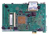
ML505
ML505 Picture Gallery
- ML505 User Guide (PDF)
- ML505 Reference Design User Guide (PDF)
- ML505 Getting Started Tutorial (PDF)
- ML505 Schematics (PDF)
- ML505 Gerber Plots (PDF)
- ML505 BOM Spreadsheet (XLS)
- ML505 Fab Drawings (ZIP)
PCB and Gerber Source Files
- ML505 Gerber Files (ZIP)
- ML505 PCB Files (Allegro 15.x) (ZIP)
- ML505 Schematic Files (Viewdraw) (ZIP)
ML505 Picture Gallery
参考设计
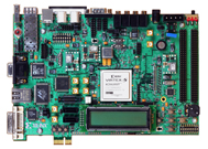
Getting Started with ML501 Demonstrations
Your ML501 Evaluation Platform is a general purpose board that ships with a number of demonstration designs pre-installed on the Compact Flash card, Platform Flash, and Linear Flash memories. The ML501 Getting Started Tutorial describes how to quickly get started using your ML501. This tutorial also contains a number of hands-on user lab exercises to help you explore the features of your ML501.
- ML501 Getting Started Tutorial (PDF)
- ML501 QuickStart (PDF)
- ML501 Lab Resources (ZIP)
ML501 Base System Builder & Reference Design Material
The Xilinx Base System Builder (BSB) wizard helps users quickly build a working embedded processing system design through an easy to use GUI interface. The XPS project created by BSB can be run as generated or further enhanced with peripherals added from the EDK IP catalog.
Please see Answer Record # 34466 for the ISE 12.1 Design Suite Known Issues.
EDK 12.1/ ISE 12.1- ML501 BSB & Reference Designs
ML501 Memory Interface Generator Design
Using the Xilinx Core Generator™ Memory Interface Generator to build a DDR2 design. Includes ChipScope™ Pro addition and testing.
- ML501 MIG Design
ML501 Configuration Methods
The ML501 can be used to demonstrate a variety of Virtex-5 configuration methods. Initial board bring-up and testing can be accomplished with the Xilinx tools, a JTAG cable, along with the bitstreams and ELF files from the ML501 standalone applications page. Subsequently, ACE files containing both hardware and software initialization components can be generated and loaded from a CompactFlash card by the onboard System ACE™ CF controller. A new Virtex-5 configuration method loads bitstreams directly from a linear flash memory device. Demonstrating the various Virtex-5 configuration methods is user-selectable through a DIP switch.
- ML501 Flash Images
- Virtex-5 Configuration User Guide (PDF)
