LT1055 - Precision, High Speed, JFET Input Operational Amplifiers
The LT1055/LT1056 JFET input operational amplifiers combine precision specifications with high speed performance.
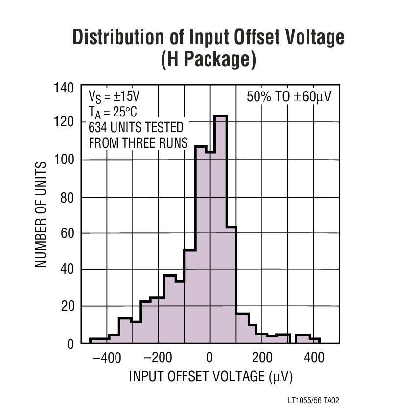
For the first time, 16V/µs slew rate and 6.5MHz gain-bandwidth product are simultaneously achieved with offset voltage of typically 50µV, 1.2µV/°C drift, bias currents of 40pA at 70°C and 500pA at 125°C.
The 150µV maximum offset voltage specification is the best available on any JFET input operational amplifier.
The LT1055 and LT1056 are differentiated by their operating currents. The lower power dissipation LT1055 achieves lower bias and offset currents and offset voltage. The additional power dissipation of the LT1056 permits higher slew rate, bandwidth and faster settling time with a slight sacrifice in DC performance.
The voltage-to-frequency converter shown below is one of the many applications which utilize both the precision and high speed of the LT1055/LT1056.
For a JFET input op amp with 23V/µs guaranteed slew rate, refer to the LT1022 data sheet.
| Part Number | Package | Temp | Price(1-99) | Price (1k)* |
|---|---|---|---|---|
| LT1055CN8#PBF | N-8 | C | $2.25 | $1.90 |
| LT1055S8#PBF | SO-8 | C | $2.67 | $2.35 |
| LT1055S8#TRPBF | SO-8 | C | $2.41 |
Demo Boards
| Part Number | Description | Price |
|---|---|---|
| DC417B | DIP8, MS8, S8, SOT23-6 | Multi-Footprint General Purpose Board for Single Op. Amp | $25.00 |
- AN10 - Methods for Measuring Op Amp Settling Time
- AN12 - Circuit Techniques for Clock Sources
- AN18 - Power Gain Stages for Monolithic Amplifiers
- AN43 - Bridge Circuits
- DN140 - Updated Operational Amplifier Selection Guide for Optimum Noise Performance
- DN15 - Noise Calculations in Op Amp Circuits
- DN3 - Operational Amplifier Selection Guide for Optimum Noise Performance
- DN6 - Operational Amplifier Selection Guide for Optimum Noise Performance
- R040 Reliability Data
- September 2009 - Consider New Precision Amplifiers for Updated Industrial Equipment Designs
- LT1055 Footprints and Symbols
- LT1055 Demo Circuit - ±120V Output Precision Op Amp
- LT1028/LT1055/LT1634 Demo Circuit - Super Low Distortion Variable Sine Wave Oscillator


