LTC1152 - Rail-to-Rail Input Rail-to-Rail Output Zero-Drift Op Amp
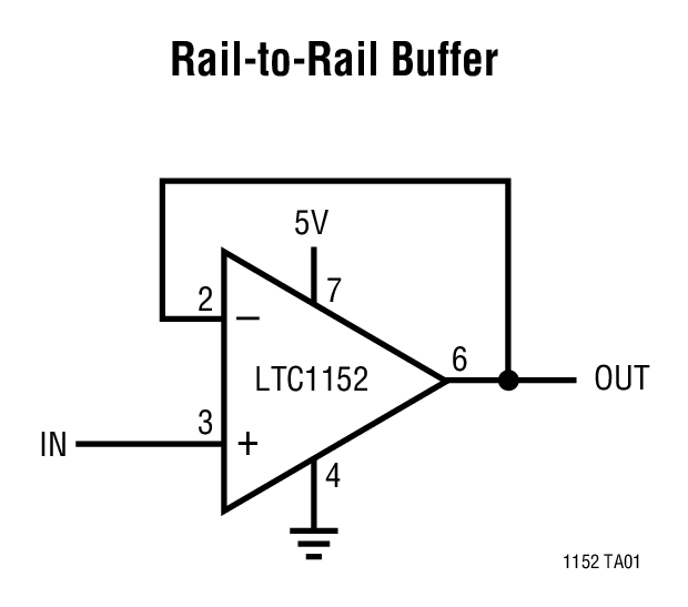
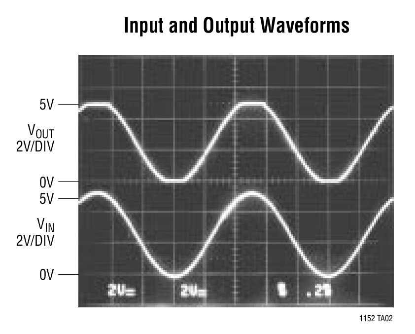
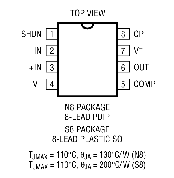
The LTC®1152 is a high performance, low power zero-drift op amp featuring an input stage that common modes to both power supply rails and an output stage that provides rail-to-rail swing, even into heavy loads. The wide in put common-mode range is achieved with a high frequency on-board charge pump. This technique eliminates the crossover distortion and limited CMRR imposed by competing technologies. The LTC1152 is a C-Load (TM) of amp, enabling it to drive any capacitive load. The LTC1152 shares the excellent DC performance specs of LTC’s other zero-drift amplifiers. Typical offset voltage is 1µVand typical offsetdrift is 10nV/°C.CMRR and PSRR are 130dB and 120dB and open-loop gain is 130dB. Input noise voltage is 2µVP-P from 0.1Hz to 10Hz. Gain-bandwidth product is 0.7MHz and slew rate is 0.5V/µs, all with product is 0.7MHz and slew rate is 0.5V/µs, all with supply current of 3.0mA max over temperature. The LTC1152 also includes a shutdown feature which drops supply current to 1µA and puts the output stage in a high impedance state. The LTC1152 is available in 8-pin PDIP and 8-pin SO packages and uses the standard op amp pinout, allowing it to be a plug-in replacement for many standard op amps.
| Part Number | Package | Temp | Price(1-99) | Price (1k)* |
|---|---|---|---|---|
| LTC1152CN8#PBF | N-8 | C | $4.00 | $3.15 |
| LTC1152CS8#PBF | SO-8 | C | $4.35 | $3.40 |
| LTC1152CS8#TRPBF | SO-8 | C | $3.46 | |
| LTC1152IN8#PBF | N-8 | I | $4.00 | $3.60 |
| LTC1152IS8#PBF | SO-8 | I | $4.80 | $3.85 |
| LTC1152IS8#TRPBF | SO-8 | I | $3.91 |
Demo Boards
| Part Number | Description | Price |
|---|---|---|
| DC417B | DIP8, MS8, S8, SOT23-6 | Multi-Footprint General Purpose Board for Single Op. Amp | $25.00 |
- LTC1152 - Rail-to-Rail Input Rail-to-Rail Output Zero-Drift Op Amp Specification Notice
- AN86 - A Standards Lab Grade 20-Bit DAC with 0.1ppm/° Drift: The Dedicated Art of Digitizing One Part Per Million
- Design Solutions 11 - Testing Linearity of the LTC2400 24-Bit No Latency Delta SigmaTM A/D Converter Help from the Nineteenth Century
- Design Solutions 4 - High Accuracy, Differential to Single-Ended Conversion for Wide Range Bipolar Input Signals Bipolar Differential to Single-Ended Converter Drives the LTC2400's Input Rail-to-Rail
- Design Solutions 5 - Low Level, High Accuracy, Bipolar Input Differential to Single-Ended Signal Conversion for 24-Bit A/D Single Supply Differential to Single-Ended Conversion Circuit Amplifies Low Level Bipolar Signals and Maintains the LTC2400's High
- R235 Reliability Data
- LTC1152 Footprints and Symbols


