NB3H83905CDGEVB:NB3H83905 CUST EVAL BOARD
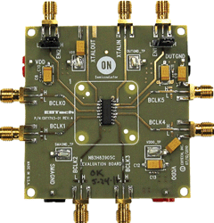
The NB3H83905CDGEVB Evaluation board is designed to provide a flexible and convenient platform to quickly program, evaluate and verify the performance and operation of the NB3H83905CDG SOIC-16 device under test. With the device removed, this NB3H83905CDGEVB Evaluation board is designed to accept a 16 Lead SOIC socket to permit use as an insertion test fixture. The NB3H83905CDG device is a 1.8 V, 2.5 V or 3.3 VVDD core Crystal input 1:6 LVTTL/LVCMOS fanout buffer with outputs powered by flexible 1.8 V, 2.5 V, or 3.3 V supply (with VDD≥VDDO). The core inputs accept a fundamental Parallel Resonant crystal from 3 MHz to 40 MHz or Single Ended LVCMOS Clock from 3 MHz to 100 MHz. Core supply must be equal or greater voltage than the output supply
特性
- Crystal source mount, or external clock source (SMA) input. One 25 Mhz crystal is supplied.
|
NB3H83905CDGEVB 实物图

|
评估板信息
| 评估板 |
状况 |
无铅(Pb-free) |
简短说明 |
所用产品 |
| NB3H83905CDGEVB |
Active |
|
NB3H83905 CUST EVAL BOARD |
NB3H83905CDG |
技术文档
