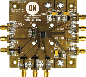
NB3N3020DTGEVB:NB3N3020 CUST EVAL BOARD
The NB3N3020DTG is a high precision, low phase noise selectable clock multiplier. The device takes a 5 - 27 MHz fundamental mode parallel resonant crystal or a 2 - 210 MHz LVCMOS single ended clock source and generates a differential LVPECL output and a single ended LVCMOS/LVTTL output at a selectable clock output frequency which is a multiple of the input clock frequency. Three tri-level (Low, Mid, High) LVCMOS/LVTTL single ended select pins set one of 26 possible clock multipliers. An LVCMOS/LVTTL output enable (OE) tri-states clock outputs when low. This device is housed in 5 mm x 4.4 mm narrow body TSSOP-16 pin package. The NB3N3020DTGEVB Evaluation board is designed to provide a flexible and convenient platform to quickly program, evaluate and verify the performance and operation of the NB3N3020DTG TSSOP-16 device under test: With the device removed, this NB3N5573DTGEVB Evaluation board is designed to accept a 16 Lead TSSOP Socket to permit use as an insertion test fixture.
特性
- Crystal mount source, or input external clock source (SMA). One 25 MHz crystal is supplied.
- A TSSOP-16 NB3N3020DTG device is solder mounted or the board may be adapted for insertion testing by adding a TSSOP-16 socket.
- Separate supply connectors for VDD, GND, and VEE (banana jacks and Anvil Clips)
|
NB3N3020DTGEVB 实物图

|
评估板信息
| 评估板 |
状况 |
无铅(Pb-free) |
简短说明 |
所用产品 |
| NB3N3020DTGEVB |
Active |
|
NB3N3020 CUST EVAL BOARD |
NB3N3020DTG, NB3N3020DTR2G |
技术文档
