NB3N502DEVB:NB3N502DEVB: 3.3 V / 5 V, 14 MHz to 190 MHz PLL Clock Multiplier Evaluation Board
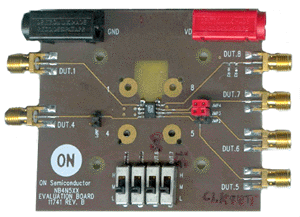
The NB3N502 Evaluation Board was designed to provide a flexible and convenient platform to quickly evaluate, characterize and verify the performance and operation of the NB3N502 PLL Clock Multiplier. The NB3N502 is a clock multiplier device that generates a low jitter, TTL/CMOS level output clock which is a precise multiple of the external input reference clock signal source. The user's manual provides detailed information on the board's contents, layout and use, and it should be used in conjunction with the NB3N502 data sheet which contains full technical details on device specifications and operation.
特性
- Fully Assembled Evaluation Board
- Accommodates the Electrical Characterization of the NB3N502 in the SOIC-8 Package
- Supports the Use of a 5 MHz to 27 MHz Through-hole or Surface Mount Crystal
- SMA Connectors are Provided for Auxiliary Input and Output Interfaces
- Incorporates Onboard Slide Switch Controlled Multiplier Select Pins, Minimizing Excess Cabling
|
NB3N502DEVB 实物图

|
评估板信息
| 评估板 |
状况 |
无铅(Pb-free) |
简短说明 |
所用产品 |
| NB3N502DEVB |
Active |
|
NB3N502DEVB: 3.3 V / 5 V, 14 MHz to 190 MHz PLL Clock Multiplier Evaluation Board |
NB3N502DG, NB3N502DR2G |
技术文档
