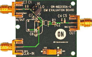
NB4N527SMNEVB:NB4N527S 3.3V 2.5Gb/s Dual AnyLevel to LVDS Reciever/Driver/Buffer/Translator w/ Input Termination Evaluation Board
The NB4N441 is a precision clock synthesizer which generates a differential LVPECL clock output frequency from 12.5 MHz to 425 MHz. A Serial Peripheral Interface (SPI) is used to configure the device to produce one of sixteen popular standard protocol output frequencies from a single 27 MHz crystal reference. The NB4N441 also has the added feature of allowing application specific output frequencies from 12.5 MHz to 425 MHz using crystals within the range of 10 MHz to 28 MHz.
特性
- Maximum Input Clock Frequency up to 1.25 GHz
- Maximum Input Data Rate up to 2.5 Gb/s
- 500 ps Maximum Propagation Delay
- 2 ps Maximum RMS Jitter
- 300 ps Maximum Rise/Fall Times
- Single Power Supply; VCC = 3.3 V +/- 10%
- Temperature Compensated TIA/EIA644 Compliant LVDS Outputs
- Internal 50 Termination Resistor per Input Pin
- GND + 50 mV to VCC 50 mV VCMR Range
|
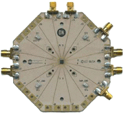
NB4N527SMNEVB 实物图

|
评估板信息
| 评估板 |
状况 |
无铅(Pb-free) |
简短说明 |
所用产品 |
| NB4N527SMNEVB |
Active |
|
NB4N527SMNEVB:NB4N527S 3.3V 2.5Gb/s Dual AnyLevel to LVDS Reciever/Driver/Buffer/Translator w/ Input Termination Evaluation Board |
NB4N527SMNG, NB4N527SMNR2G |
技术文档
