NB4N855SMEVB:NB4N855SM 3.3V 2.5Gb/s Dual AnyLevelTM to LVDS Reciever/Driver/Buffer/Translator Evaluation Board
The NB4N855SMEVB has been developed as a convenience for the customers interested in performing their own device engineering assessment. This evaluation board provides a high bandwidth 50 ohm controlled impedance environment. The NB4N855SMEVB Manual contains appropriate lab setup, assembly instructions and bill of materials.
特性
- Guaranteed Input Clock Frequency up to 1.0 GHz
- Guaranteed Input Data Rate up to 1.5 Gb/s
- 490 ps Maximum Propagation Delay
- 1.0 ps Maximum RMS Jitter
- 180 ps Maximum Rise/Fall Times
- Single Power Supply; VCC = 3.3 V 10%
- Temperature Compensated TIA/EIA-644 Compliant LVDS Outputs
- GND + 50 mV to VCC - 50 mV VCMR Range
|
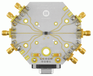
NB4N855SMEVB 实物图

|
评估板信息
| 评估板 |
状况 |
无铅(Pb-free) |
简短说明 |
所用产品 |
| NB4N855SMEVB |
Active |
|
NB4N855SMEVB:NB4N855SM 3.3V 2.5Gb/s Dual AnyLevelTM to LVDS Reciever/Driver/Buffer/Translator Evaluation Board |
NB4N855SMR4G |
技术文档
