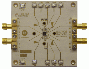
NB7L216MNEVB:NB7L216 2.5V/3.3V 12 Gb/s Multi Level Clock/Data Input to RSECL High Gain Receiver/Buffer/Translator with Internal Termination Evaluation Board
The NB7L216 evaluation board is implemented in two layers and provides a high bandwidth 50 Ω controlled impedance environment for higher performance. First layer or primary trace layer is 5 mils thick Rogers RO6002 material, which is engineered to have equal electrical length on all signal traces from NB7L216 device to the sense output. The second layer is 32 mils thick copper ground plane. For standard lab setup and test, a split (dual) power supply is required enabling the 50 ohm impedance in the scope to be used as termination of the ECL signals (VTT = VCC - 2.0 V, in split power supply setup, VTT is the system ground).
特性
- High Gain of 35 dB from DC to 7 GHz
- High IIP3: 0dB
- 20 mV Minimum Input Voltage Swing
- Maximum Input Clock Frequency > 8.5 GHz Typical
- Maximum Input Data Rate > 12 Gb/s
- 120 ps Typical Propagation Delay
- 30 ps Typical Rise and Fall Times
- RSECL Output Level (400 mV Peak-to-Peak Output),Differential Output Only
- 50 Internal Input Termination Resistors (temp-coefficient of < 6 mΩ/C)
- Functionally Compatible with Existing 2.5 V / 3.3 V LVEL, LVEP, EP, and SG Devices
- Vbb ECL Reference Voltage Output
- Test Equipment First Stage Amplifier
- Data communications Post Amplifier
|
NB7L216MNEVB 实物图

|
评估板信息
| 评估板 |
状况 |
无铅(Pb-free) |
简短说明 |
所用产品 |
| NB7L216MNEVB |
Active |
 |
NB7L216MNEVB:NB7L216 2.5V/3.3V 12 Gb/s Multi Level Clock/Data Input to RSECL High Gain Receiver/Buffer/Translator with Internal Termination Evaluation Board |
NB7L216MNG, NB7L216MNR2G |
技术文档
