NCP3065D2SLDGEVB:SEPIC LED DRV 350MA
This circuit is intended for driving high power LEDs. It is designed for such wide input nominal 12 Vdc applications as automotive and low voltage lighting (12 Vdc/12 Vac). An optional dimming PWM input is included. The circuit is based on NCP3065 operation at 250 kHz in a non-isolated configuration. The primary advantages of this circuit are in the wide input voltage range, wide output voltage range, and in its high efficiency. A pulse feedback resistor (R8) is used to vary the slope of the oscillator ramp, achieving duty cycle control and steady switching frequency over a wide input voltage range.
技术特性
- Buck-Boost operation
- Wide input and output operation voltage
- Regulated output current
- Dimming
- High frequency operation
- Minimal input and output current ripple
- Open LED protection
- Output short circuit protection
|
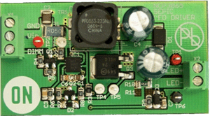
NCP3065D2SLDGEVB 实物图

|
评估板信息
| 评估板 |
状况 |
无铅(Pb-free) |
简短说明 |
所用产品 |
| NCP3065D2SLDGEVB |
Active |
 |
SEPIC LED DRV 350MA |
NCV3065MNTXG |
技术文档