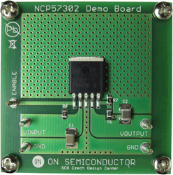
NCP57302DSADGEVB:3A ADJ VLDO REG DB
The NCP57302 is a high precision, very low dropout (VLDO), low minimum input voltage and low ground current positive voltage regulator that is capable of providing an output current in excess of 3.0 A with a typical dropout voltage of 315 mV at 3.0 A load current and input voltage from 1.8 V and up. The device is stable with ceramic output capacitors. The device can withstand up to 18 V max input voltage. Internal protection features consist of output current limiting, built-in thermal shutdown and reverse output current protection. Logic level enable pin is available. The NCP57302 is an adjustable voltage device and is available in D2PAK-5 package.
特性
- Input Voltage Range from 2.7 V to 12 V (Limited to 5.5 V in case the Single Output Buffer is powered too.)
- Low Quiescent Current, Typical 2.7 µA
- Output Current up to 150 mA
- Precision 3% at Ta = 25°C
- Internal Thermal Shutdown Protection
- Current Limiting
- NCV Prefix for Automotive and Other Applications Requiring Site and Control Changes
- These are Pb-Free Devices
|
应用
- Battery Powered Instruments
- Hand-Held Instruments
- Camcorders and Cameras
NCP57302DSADGEVB 实物图

|
评估板信息
| 评估板 |
状况 |
无铅(Pb-free) |
简短说明 |
所用产品 |
| NCP57302DSADGEVB |
Active |
 |
3A ADJ VLDO REG DB |
NCP57302DSADJR4G |
技术文档