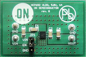
NCP692MN50T2GEVB:NCP692 5.0V EVAL BOARD
The NCP692 CMOS LDO family provides 1 A of output current with enhanced ESD in fixed output voltage options from 1.5 V to 5.0 V. These devices are designed for space constrained and portable battery powered applications and offer additional features such as low Dropout Voltage, high Power Supply Rejection Ratio (PSRR), low Quiescent and Ground Current consumption, low Noise operation, Short Circuit and Thermal Protection. NCP692 is designed to be used with low cost ceramic capacitors and the minimum value of 1µF output capacitance is required. The NCP692 device is equipped with Active High Enable pin, Active Output Discharge, Current Limit and Thermal Shutdown Protection. Finally the Surface Mount DFN3x3 package with Expose Pad allows saving PCB space and effectively dissipating heat through the PCB copper area. This demonstration board operates from a dc input voltage VIN < 6V and produces fixed output voltage given by the NCP692 internal voltage divider. External waveform generator could be connected to the EN (Enable) pin in order to verify the ON/OFF operation.
特性
|
NCP692MN50T2GEVB 实物图

|
评估板信息
| 评估板 |
状况 |
无铅(Pb-free) |
简短说明 |
所用产品 |
| NCP692MN50T2GEVB |
Active |
 |
NCP692 5.0V EVAL BOARD |
NCP692MN50T2G |
技术文档