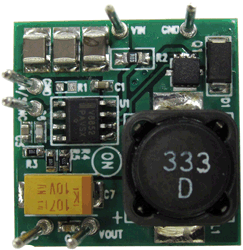
NCV8853GEVB:NCV8852 EVAL BOARD
The NCV8852 demonstration board provides a convenient way to evaluate and integrate a complete high-efficiency non-synchronous buck converter design. No additional components are required, other than dc supplies for the input voltage and enable pin. The board can also be connected to an external clock source to synchronize the switching frequency. The board is configured for a 5.0 V output with a 170 kHz switching frequency and a 3 A current limit, intended for applications requiring 2 A of current. Modifying the NCV8852 demonstration board for different output voltage, switching frequency, or current limit is straightforward, requiring minimal component changes.
|
NCV8853GEVB 实物图

|
评估板信息
| 评估板 |
状况 |
无铅(Pb-free) |
简短说明 |
所用产品 |
| NCV8853GEVB |
Active |
 |
NCV8852 EVAL BOARD |
NCV8852DR2G |
技术文档
