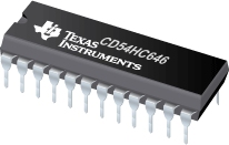
CD54HC646 具有三态输出的高速 CMOS 逻辑八路反向总线收发器

The CD54HC646 and CD74HCT646 consist of bus-transceiver circuits with 3-state outputs, D-type flip-flops, and control circuitry arranged for multiplexed transmission of data directly from the input bus or from the internal registers. Data on the A or B bus is clocked into the registers on the low-to-high transition of the appropriate clock (CLKAB or CLKBA) input. Figure 1 illustrates the four fundamental bus-management functions that can be performed with these devices.
Output-enable (OE\) and direction-control (DIR) inputs control the transceiver functions. In the transceiver mode, data present at the high-impedance port can be stored in either or both registers.
The select-control (SAB and SBA) inputs can multiplex stored and real-time (transparent mode) data
| CD54HC646 | |
| Voltage Nodes (V) | 6, 5, 2 |
| Technology Family | HC |
| Rating | Military |
CD54HC646 特性
- 2-V to 6-V VCC Operation (CD54HC646)
- 4.5-V to 5.5-V VCC Operation (CD74HCT646)
- Wide Operating Temperature Range of –55°C to 125°C
- Balanced Propagation Delays and Transition Times
- Standard Outputs Drive Up To 15 LS-TTL Loads
- Significant Power Reduction Compared to LS-TTL Logic ICs
- Inputs Are TTL-Voltage Compatible (CD74HCT646)
- Independent Registers for A and B Buses
- Multiplexed Real-Time and Stored Data
- True Data Paths
CD54HC646 芯片订购指南
| 器件 | 状态 | 温度 | 价格(美元) | 封装 | 引脚 | 封装数量 | 封装载体 | 丝印标记 |
| 5962-8688501JA | ACTIVE | -55 to 125 | 14.53 | 1ku | CDIP (J) | 24 | 1 | TUBE | |
| CD54HC646F3A | ACTIVE | -55 to 125 | 14.53 | 1ku | CDIP (J) | 24 | 1 | TUBE |
CD54HC646 应用手册
CD54HC646 质量与无铅数据
| 器件 | 环保计划* | 铅/焊球涂层 | MSL 等级/回流焊峰 | 环保信息与无铅 (Pb-free) | DPPM / MTBF / FIT 率 |
| 5962-8688501JA | TBD | Call TI | Call TI | 5962-8688501JA | 5962-8688501JA |
| CD54HC646F3A | TBD | Call TI | N/A for Pkg Type | CD54HC646F3A | CD54HC646F3A |
CD54HC646 应用技术支持与电子电路设计开发资源下载
- CD54HC646 数据资料 dataSheet 下载.PDF
- TI 德州仪器触发器/锁存器/寄存器产品选型与价格 . xls
- Shelf-Life Evaluation of Lead-Free Component Finishes (PDF 1305 KB)
- Understanding and Interpreting Standard-Logic Data Sheets (PDF 857 KB)
- TI IBIS File Creation, Validation, and Distribution Processes (PDF 380 KB)
- Implications of Slow or Floating CMOS Inputs (PDF 101 KB)
- CMOS Power Consumption and CPD Calculation (PDF 89 KB)
- Designing With Logic (PDF 186 KB)
- Live Insertion (PDF 150 KB)
- Input and Output Characteristics of Digital Integrated Circuits (PDF 1708 KB)
- Using High Speed CMOS and Advanced CMOS in Systems With Multiple Vcc (PDF 43 KB)
- HiRel Unitrode Power Management Brochure (PDF 206 KB)
- LOGIC Pocket Data Book (PDF 6001 KB)
- HiRel Unitrode Power Management Brochure (PDF 206 KB)
- Logic Cross-Reference (PDF 2938 KB)
