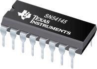
SN54145 BCD 至十进制解码器/驱动器
 These monolithic BCD-to-decimal decoder/drivers consist of eight inverters and ten four-input NAND gates. The inverters are connected in pairs to make BCD input date available for decoding by the NAND gates. Full decoding of valid BCD input logic ensures that all outputs remain off for all invalid binary input conditions. These decoders feature high-performance,
n-p-n output transistors designed for use as indicator/relay drivers or as open-collector logic-circuit drivers. Each of the high-breakdown output transistors (15 volts) of the SN54145, SN74145, or SN74LS145 will sink up to 80 milliamperes of current. Each input is one Series 54/74 or Series 54LS/74LS standard load, respectively. Inputs and outputs are entirely compatible for use with TTL or DTL logic curciuts, and the outputs are compatible for interfacing with most MOS integrated circuits
| SN54145 | |
| Rating | Military |
| Technology Family | TTL |
SN54145 特性
- Full Decoding of Input Logic
- SN54145, SN74145, and SN74LS145 Have 80-mS Sink-current Capability
- All Outputs Are Off for Invalid BCD Input Conditions
- Low Power Dissipation of 'LS145 . . . 35 mW Typical
SN54145 芯片订购指南
| 器件 | 状态 | 温度 | 价格 | 封装 | 引脚 | 封装数量 | 封装载体 | 丝印标记 |
| SNJ54145J | ACTIVE | -55 to 125 | 5.99 | 1ku | CDIP (JT) | 16 | 1 | TUBE |
SN54145 质量与无铅数据
| 器件 | 环保计划* | 铅/焊球涂层 | MSL 等级/回流焊峰 | 环保信息与无铅 (Pb-free) | DPPM / MTBF / FIT 率 |
| SNJ54145J | TBD | A42 | N/A for Pkg Type | SNJ54145J | SNJ54145J |
SN54145 应用技术支持与电子电路设计开发资源下载
- SN54145 数据资料 dataSheet 下载.PDF
- TI 德州仪器MSI 功能产品选型与价格 . xls
- Logic Guide 2009 (PDF 4263 KB)
- Shelf-Life Evaluation of Lead-Free Component Finishes (PDF 1305 KB)
- Understanding and Interpreting Standard-Logic Data Sheets (PDF 857 KB)
- TI IBIS File Creation, Validation, and Distribution Processes (PDF 380 KB)
- Implications of Slow or Floating CMOS Inputs (PDF 101 KB)
- CMOS Power Consumption and CPD Calculation (PDF 89 KB)
- Designing With Logic (PDF 186 KB)
- Live Insertion (PDF 150 KB)
- Input and Output Characteristics of Digital Integrated Circuits (PDF 1708 KB)
- Using High Speed CMOS and Advanced CMOS in Systems With Multiple Vcc (PDF 43 KB)
- HiRel Unitrode Power Management Brochure (PDF 206 KB)
- LOGIC Pocket Data Book (PDF 6001 KB)
- HiRel Unitrode Power Management Brochure (PDF 206 KB)
- Logic Cross-Reference (PDF 2938 KB)
