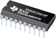
SN54AC244-SP 具有三态输出的八路缓冲器/驱动器

These octal buffers and line drivers are designed specifically to improve the performance and density of 3-state memory address drivers, clock drivers, and bus-oriented receivers and transmitters.
The ’AC244 devices are organized as two 4-bit buffers/drivers with separate output-enable (OE)\ inputs. When OE\ is low, the device passes noninverted data from the A inputs to the Y outputs. When OE\ is high, the outputs are in the high-impedance state.
To ensure the high-impedance state during power up or power down, OE\ should be tied to VCC through a pullup resistor; the minimum value of the resistor is determined by the current-sinking capability of the driver
|
SN54AC244-SP |
| Voltage Nodes (V) |
5, 3.3 |
| Vcc range (V) |
2.0 to 6.0 |
| Input Level |
CMOS |
| Output Level |
CMOS |
| No. of Outputs |
8 |
| Logic |
True |
| Technology Family |
AC |
| Rating |
Space |
| Pin/Package |
20CDIP, 20CFP |
SN54AC244-SP 特性
- 2-V to 6-V VCC Operation
- Inputs Accept Voltages to 6 V
- Max tpd of 7.5 ns at 5 V
SN54AC244-SP 芯片订购指南
| 器件 |
状态 |
温度 |
价格(美元) |
封装 | 引脚 |
封装数量 | 封装载体 |
丝印标记 |
| 5962-8755201VRA |
ACTIVE |
-55 to 125 |
56.95 | 100u |
CDIP (J) | 20 |
1 | TUBE |
|
| 5962-8755201VSA |
ACTIVE |
-55 to 125 |
98.05 | 100u |
CFP (W) | 20 |
1 | TUBE |
|
SN54AC244-SP 应用手册
SN54AC244-SP 质量与无铅数据
| 器件 |
环保计划* |
铅/焊球涂层 |
MSL 等级/回流焊峰 |
环保信息与无铅 (Pb-free) |
DPPM / MTBF / FIT 率 |
| 5962-8755201VRA |
TBD |
A42 |
N/A for Pkg Type |
5962-8755201VRA |
5962-8755201VRA |
| 5962-8755201VSA |
TBD |
A42 |
N/A for Pkg Type |
5962-8755201VSA |
5962-8755201VSA |
SN54AC244-SP 应用技术支持与电子电路设计开发资源下载
- SN54AC244-SP 数据资料 dataSheet 下载.PDF
- TI 德州仪器缓冲器、驱动器/收发器产品选型与价格 . xls
- (选择指南)逻辑器件指南 2009 (Rev. Z)
- (用户指南)LOGIC Pocket Data Book
- (用户指南)Signal Switch Data Book
- Logic Cross-Reference (PDF 2938 KB)

