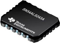
SN54ALS243A 具有三态输出的八路总线收发器

These quadruple bus transceivers are designed for asynchronous two-way communication between data buses. The control-function implementation allows for maximum flexibility in timing. These devices allow data transmission from the A bus to the B bus or from the B bus to the A bus depending upon the logic levels at the output-enable (OEBA and ) inputs. The output-enable inputs can be used to disable the device so that the buses are effectively isolated.
The dual-enable configuration gives the quadruple bus transceivers the capability to store data by simultaneously enabling OEBA and . Each output reinforces its input in this transceiver configuration. When both control inputs are enabled and all other data sources to the two sets of bus lines are at high impedance, both sets of bus lines (eight in all) retain their states
| SN54ALS243A | |
| Voltage Nodes (V) | 5 |
| Vcc range (V) | 4.5 to 5.5 |
| Input Level | TTL |
| Output Level | TTL |
| No. of Outputs | 4 |
| Logic | True |
| Rating | Military |
| Technology Family | ALS |
SN54ALS243A 特性
- Two-Way Asynchronous Communication Between Data Buses
- pnp Inputs Reduce dc Loading
- Package Options Include Plastic Small-Outline (D) Packages, Ceramic Chip Carriers (FK), and Standard Plastic (N) and Ceramic (J) 300-mil DIPs
SN54ALS243A 芯片订购指南
| 器件 | 状态 | 温度 | 价格(美元) | 封装 | 引脚 | 封装数量 | 封装载体 | 丝印标记 |
| 84013022A | ACTIVE | -55 to 125 | 17.37 | 1ku | LCCC (FK) | 20 | 1 | TUBE | |
| 8401302CA | ACTIVE | -55 to 125 | 6.83 | 1ku | CDIP (J) | 14 | 1 | TUBE | |
| 8401302DA | ACTIVE | -55 to 125 | 10.07 | 1ku | CFP (W) | 14 | 1 | TUBE | |
| SNJ54ALS243AFK | ACTIVE | -55 to 125 | 17.37 | 1ku | LCCC (FK) | 20 | 1 | TUBE | |
| SNJ54ALS243AJ | ACTIVE | -55 to 125 | 6.83 | 1ku | CDIP (J) | 14 | 1 | TUBE | |
| SNJ54ALS243AW | ACTIVE | -55 to 125 | 10.07 | 1ku | CFP (W) | 14 | 1 | TUBE |
SN54ALS243A 应用手册
SN54ALS243A 质量与无铅数据
| 器件 | 环保计划* | 铅/焊球涂层 | MSL 等级/回流焊峰 | 环保信息与无铅 (Pb-free) | DPPM / MTBF / FIT 率 |
| 84013022A | TBD | Call TI | Call TI | 84013022A | 84013022A |
| 8401302CA | TBD | Call TI | Call TI | 8401302CA | 8401302CA |
| 8401302DA | TBD | Call TI | Call TI | 8401302DA | 8401302DA |
| SNJ54ALS243AFK | TBD | POST-PLATE | N/A for Pkg Type | SNJ54ALS243AFK | SNJ54ALS243AFK |
| SNJ54ALS243AJ | TBD | A42 | N/A for Pkg Type | SNJ54ALS243AJ | SNJ54ALS243AJ |
| SNJ54ALS243AW | TBD | A42 | N/A for Pkg Type | SNJ54ALS243AW | SNJ54ALS243AW |
SN54ALS243A 应用技术支持与电子电路设计开发资源下载
- SN54ALS243A 数据资料 dataSheet 下载.PDF
- TI 德州仪器触发器/锁存器/寄存器产品选型与价格 . xls
- (用户指南)LOGIC Pocket Data Book
- (用户指南)Signal Switch Data Book
- (用户指南)LVC and LV Low-Voltage CMOS Logic Data Book
- (选择指南)逻辑器件指南 2009 (Rev. Z)
- (选择指南)小尺寸逻辑器件指南 (Rev. D)
- 2008年第一季度通信基础设施方案指南 (Rev. G)
- Communications Infrastructure Solutions Guide 1Q2010
- Design Summary for WCSP Little Logic
- Standard Linear & Logic for PCs, Servers & Motherboards
- STANDARD LINEAR AND LOGIC FOR DVD/VCD PLAYERS
- Military Low Voltage Solutions
- Low-Voltage Logic (LVC) Designer's Guide
- Logic Cross-Reference
